Newsroom
RF Power Amplifiers Part 2: Switch-Mode Amplifiers and Linearity Explained
Class D: The Art of Switching in Voltage Mode
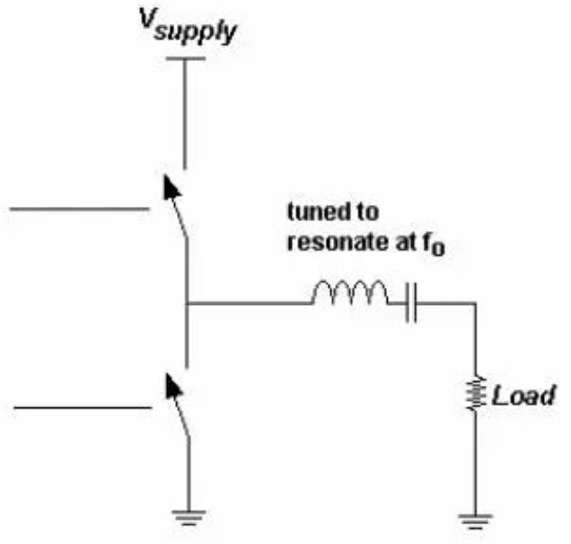
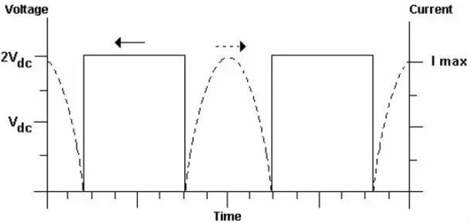
Class D amplifiers employ two or more transistors acting as switches to create a square‑wave drain voltage waveform. The output passes through a series‑tuned filter, which allows only the fundamental component to reach the load. This produces a half‑sine current waveform and a square voltage waveform.
- Zero voltage and current overlap: In theory, the voltage and current waveforms never overlap in the time domain—either there’s voltage with no current, or current with no voltage, so no switching loss.
- Load reactance doesn’t reduce efficiency: The unique advantage of Class D is that even if the load has reactance, the efficiency won’t drop.
- Hard to implement: Especially at high frequencies, switch availability, parasitic capacitance, and lead inductance all cause losses.
- No true Class D: In reality, there’s no perfect Class D amplifier, because the switch resistance isn’t zero and there are capacitive and inductive parasitics.
Class E: The Ultimate Pursuit of Single-Tube Switches
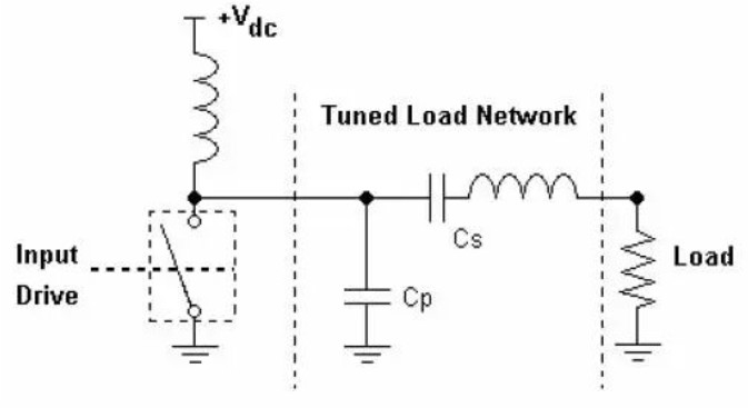
A Class E amplifier uses one transistor as a switch. DC and RF currents charge the parallel capacitor Cp — including the transistor’s internal capacitance Co — to form the drain‑voltage waveform. An optimized Class E design demands zero drain voltage and zero voltage slope at the instant the transistor turns on.
- Zero Voltage Switching (ZVS): Eliminates energy loss during voltage drop, achieving theoretically 100% efficiency.
- Eliminates charging loss: Overcomes energy loss when charging the drain capacitor in Class D amplifiers.
- RF choke: The RFC should be large enough to let only DC current Idc through.
- High-Q output circuit: An output circuit made of Ls and Cs with a high enough Q value to filter out all harmonics and keep only the fundamental frequency.
- Frequency limit: Determined by the capacitor Cs required by the output matching circuit—the bigger the capacitor, the lower the frequency limit.
High-frequency, high-power Class D amplifiers need higher current density because the switch’s cross-sectional area directly corresponds to the device’s internal capacitance.
Class F: The Art of Harmonic Shaping
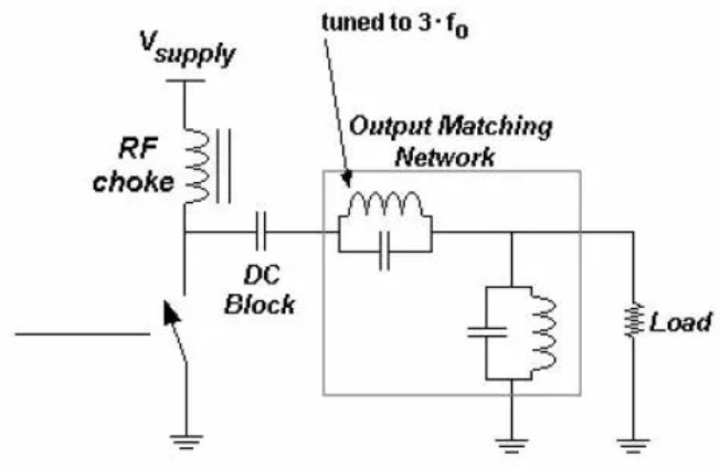
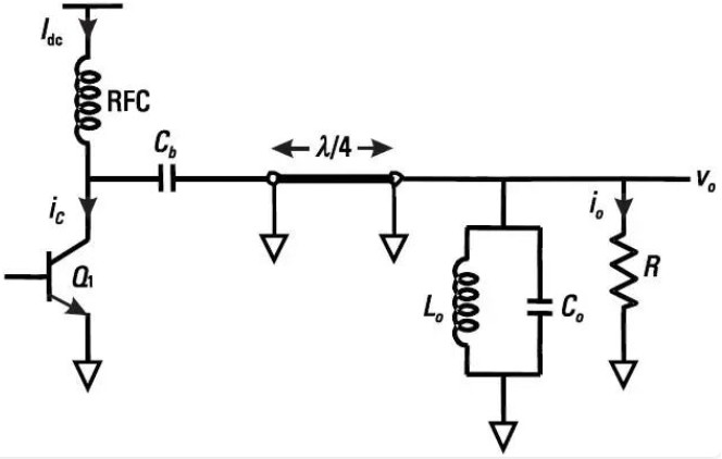
Class F amplifiers shape the drain waveform using harmonic resonators in the output network. Odd harmonics are added to the voltage waveform to approximate a square wave, and even harmonics are injected into the current waveform to form a near half‑sine wave.
- Harmonic Impedance Control:
- For odd harmonics (3f, 5f…), a high impedance (open circuit) is needed.
- For even harmonics (2f, 4f…), a low impedance (short circuit) is needed.
- λ/4 Transmission Line Solution: A quarter-wave transmission line can turn an open circuit into a short circuit, and a short circuit into an open circuit. Combined with an LC resonator, it achieves precise harmonic control.
- Theoretical Efficiency: Classic Class E is 88.4%; with infinite harmonic tuning, it can reach 100%.
- Actual Efficiency: About 72% (limited by the difficulty of achieving open-circuit termination).
- Design Challenges: Output matching network design is complex, and open-circuit termination is particularly difficult at high frequencies and high power.
Quick Reference Comparison Table for Switch-Type Power Amplifiers
| Amplifier Type | Architecture | Voltage Waveform | Current Waveform | Theoretical Efficiency | Features |
| Class D | Dual Transistor Push-Pull | Square Wave | Half-Sine | 100% | Switch-mode, Series Filtering |
| Class E | Single Transistor | Zero Voltage Slope | Half-Sine | 100% | Zero-Voltage Switching, Soft Switching |
| Class F | Harmonic Shaping | Square Wave with Odd Harmonics | Half-Sine with Even Harmonics | 88.4% | λ/4 Line, Harmonic Tuning |
Amplifier Linearity: Intermodulation Distortion and Key Metrics
When two or more signals are input into an amplifier at the same time, the intermodulation components (IM) that are produced are key to measuring linearity. These components come from combinations of the fundamental signals and their harmonics.
Cross-modulation component patterns (two-tone signals f1, f2)
Fundamental components: f1, f2
2nd-order components: 2f1, 2f2, f1±f2 (boost 2dB/1dB input)
3rd-order components: 3f1, 3f2, 2f1±f2, 2f2±f1 (boost 3dB/1dB input) ⭐Most important
5th-order components: 5f1, 5f2, 3f1±2f2, 3f2±2f1 (boost 5dB/1dB input)
1dB Compression Point (P1dB)
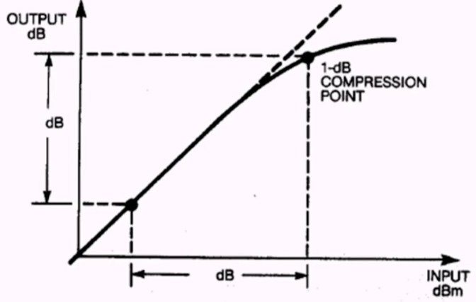
When the input power increases to a certain level, the amplifier’s gain starts to compress — the output no longer grows linearly. The 1dB compression point is defined as the output power point when the gain drops by 1dB. This is the tipping point where the amplifier goes from the linear region to the nonlinear region.
AM-AM and AM-PM Distortion
- AM-AM distortion: When the amplitude of the input signal changes, the output amplitude can’t respond linearly (gain compression/expansion).
- AM-PM distortion: When the amplitude of the input signal changes, the output phase shifts. This directly reflects the power amplifier’s ‘memory effect’—changes in low-frequency envelope impedance can affect high-frequency phase.
NPR Noise Power Ratio Test
NPR (Noise Power Ratio) is an effective way to evaluate the linearity of a broadband signal. You dig a ‘valley’ in the noise floor, then after passing it through an amplifier, you measure how much the valley gets filled in—the more it fills, the worse the linearity.
CCDF Peak Factor Measurement
The CCDF (complementary cumulative distribution function) shows the percentage of time a signal’s peak power exceeds its average power. Signals with a high PAPR (like OFDM) place huge demands on the linearity of power amplifiers—the amp has to operate with a significant power back-off to avoid distortion.
Conclusion
Switch‑mode Class D, E and F power amplifiers use transistor switching to achieve high theoretical efficiency, differing from linear Class A/AB/B/C topologies. Class D adopts dual push‑pull switches; Class E delivers zero‑voltage soft‑switching with a single‑transistor resonant circuit; Class F shapes drain waveforms via harmonic control and λ/4 transmission lines. Practical performance is constrained by component parasitics and high‑frequency losses.
As switch‑mode PAs are inherently non‑linear, engineers must assess linearity metrics: intermodulation distortion, P1dB, AM‑AM / AM‑PM distortion, NPR and CCDF, especially for high‑PAPR wideband signals. No single topology fits all scenarios. Select amplifiers based on frequency, output power, harmonic and linearity requirements to balance efficiency and linearity for RF, radar and communication systems.
Contact ZR Hi‑tech for custom RF power amplifier solutions.