Newsroom
Why Do RF Power Amplifiers Require Biasing? A Practical Guide
Open any RF circuit textbook or engineering handbook, and you will frequently see “bias circuit not shown” on many schematics. This gives the impression that biasing is only a minor secondary detail. In reality, the bias network is one of the most critical yet often overlooked parts of RF circuit design. It defines how an RF power amplifier performs across changing temperatures and RF‑driving conditions. While an RF transistor’s DC operating point is usually configured independently from the RF design, its quality directly affects: Power efficiency, stability, noise performance, thermal runaway protection.
So, why do transistors definitely need a DC bias circuit? There are two main reasons: simplifying power supply and preventing thermal runaway.
RF Power Amplifier Bias Types: A / AB / B / C Explained
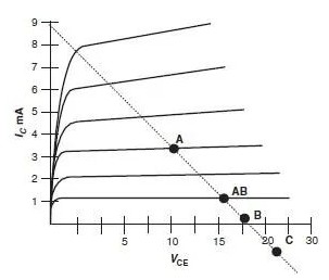
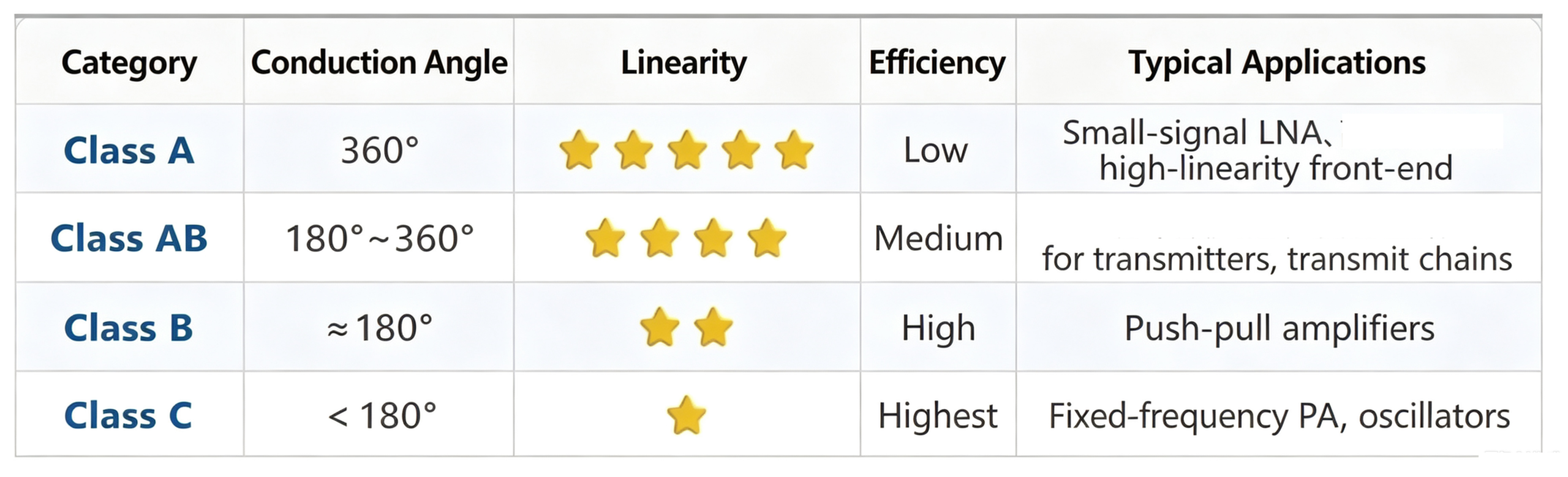
Different bias levels determine how a transistor operates. In the RF field, the most commonly used bias types are four: Class A, Class AB, Class B, and Class C. The main difference between them lies in where the transistor’s quiescent current ICQ is set.
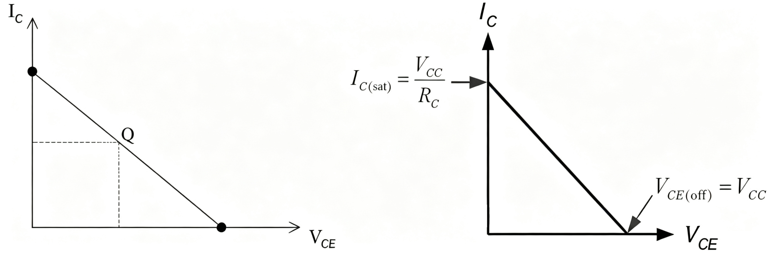
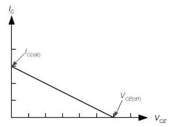
To understand this, we first need to introduce a key concept—the quiescent point. When a BJT has no AC signal input, it has specific DC values for IC and VCE, which correspond to a fixed point on the DC load line, called ICQ.
Class A Always on, The King of Linearity
Class A amplifiers stay on throughout the entire signal cycle. They’re usually used for small-signal, non-power applications. Some of their features are:
- They need a constant current bias source to lock the operating point, are unaffected by RF drive and output changes
- Require some form of feedback to keep the output current stable
- Have excellent linearity but low efficiency—because a lot of power is spent just maintaining the constant current
- Ideal for front-end amplification situations where linearity and low noise are super important
Class AB Compromise, Balancing Linearity and Efficiency
You just need to slightly lower the ICQ to transition from Class A to Class AB. It’s the most commonly used compromise in engineering:
- Efficiency is better than Class A, but output distortion is higher (because the signal waveform gets clipped)
- It requires some form of biasing, the operating point will shift with RF drive
- Need ‘open-loop’ circuit design with compensation for environmental temperature changes
Class B Conducts for Half the Cycle, Making It a Good Match For a Push-pull Setup
The quiescent current of Class B is set to zero—transistors only conduct during half of the input signal cycle. They’re usually used in pairs (push-pull configuration), which is efficient but has noticeable crossover distortion. Similar to Class AB, it also requires proper biasing and temperature compensation.
Class C Has The Highest Efficiency and The Smallest Conduction Angle
Class C usually requires applying a negative bias to the transistor—or more commonly, just grounding the base with an inductor or resistor is enough to maintain the correct conduction angle. It’s super efficient, but the linearity is the worst, mainly used in power amplification scenarios at fixed frequencies.
The Two Key Considerations For BJT Biasing
Consideration 1: The trade-off Between fT and Noise
Device datasheets usually show a curve of fT (transition frequency) versus collector current. There’s a classic trade-off here: aiming for high gain versus low noise.
Plus, the bias point has to make sure the input signal doesn’t push the collector current out of its linear range—otherwise, the signal hits saturation and gets seriously distorted. And if the amplifier has to operate over a range of temperatures, the bias network needs to keep the DC operating point steady despite temperature changes.
Consideration 2: ΔVBE and Δβ Caused by Temperature
There are two transistor internal parameters that significantly affect the stability of the DC bias point:
① VBE temperature drift: The base-emitter voltage VBE drops as the temperature rises, at a rate of about −2.5 mV/°C. This means higher temperature → lower VBE → higher base current → higher collector current. However, the voltage drop VE across the emitter resistor RE provides some negative feedback that helps suppress this—if VE increases, it in turn suppresses IC from rising.
② β (hFE) temperature drift: The DC current gain β usually increases with temperature at a rate of about 0.5%/°C, which further aggravates the instability of the collector current.
Key Finding: hFE Differences Don’t Affect RF Performance
BJTs are often used as low-cost, low-noise amplifiers (LNAs). With minimal matching networks, a BJT can achieve RF performance far beyond that of MMICs. But the device’s DC parameters are heavily influenced by process variations—the hFE of the same model can differ by up to 3:1.
Breaking Down the Four Classic Bias Schemes One by One
Base-biased Emitter Feedback
This is one of the most classic bias topologies. The circuit structure is simple: the base resistor RB, the base-emitter voltage drop VBE (about 0.7V), and the emitter resistor RE are connected in series.
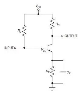
Temperature Stabilization Principle (Negative Feedback Loop): When the temperature rises → collector current IC increases → current through RE increases → voltage across RE, VE, rises → voltage margin left for RB decreases → base current IB drops → IC falls back → achieving automatic stabilization
The capacitor CE in the circuit is connected across RE, and its function is to bypass the RF signal—preventing RE from causing excessive negative feedback that would degrade RF gain.
Diode Temperature Compensation
If you want better temperature compensation, the most common method is diode temperature compensation. You attach two diodes, D1 and D2, to the transistor’s heat sink or the device itself so they can precisely track the transistor’s internal temperature changes.
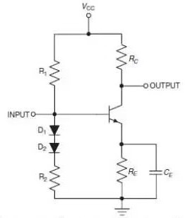
How it works: When the temperature goes up, the internal resistance of the diode drops → the forward voltage drop decreases → the VBE of the transistor is pulled down accordingly → this suppresses the increase in collector current caused by the temperature. Essentially, the negative temperature coefficient of the diode cancels out the negative temperature coefficient of the transistor, achieving accurate temperature compensation.
Collector-feedback Bias
This is a very low-cost biasing scheme, suitable for RF and microwave circuits, but its thermal stability isn’t as good as the first two. The whole circuit only needs two resistors and one active device, and since the emitter is directly grounded, the lead inductance is minimal—which is a big plus at high frequencies.
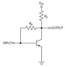
Principle of temperature stabilization: When the temperature rises → the transistor tends to conduct more current (IC increases). Note: The base resistor RB is connected directly to the collector (not the power supply), so when IC increases → more voltage drops across the collector resistor → collector voltage drops → voltage drop across RB decreases → base current IB decreases. IB decreases → IC drops back → automatic stabilization.
Class C Biasing Method
For BJT power transistors, Class C amplifiers usually offer three biasing techniques: signal bias, external bias, and self-bias. The most common case is that the Class C transistor doesn’t apply any bias to the base at all. But to prevent instability in BJT power devices, it’s recommended to ground the base through a low-Q choke and put a ferrite bead on the grounded end of the choke.
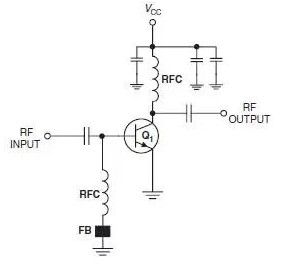
The principle of signal bias is that the amplitude of the RF input signal is large enough to overcome zero bias (or negative bias), allowing the transistor to conduct only near the signal peaks, thereby achieving a very small conduction angle and very high efficiency. Another, less commonly used method is external bias.
The external bias circuit uses a negative power supply to provide bias to the base, while the positive power supply is for the collector circuit. The RF choke (RFC) presents a high impedance at RF frequencies, preventing RF signals from mixing into the bias supply. This method allows for more precise control of the conduction angle and is suitable for situations that have strict requirements for efficiency and output power.
Conclusion
Proper DC biasing is easy to overlook on RF‑schematic diagrams, yet it largely defines power‑amplifier real‑world performance. It governs power efficiency, linearity, stability, noise and thermal safety, and directly counteracts temperature‑driven drift of VBE and β in BJT transistors.
Class A, AB, B and C amplifiers differ fundamentally by quiescent‑current setting and conduction angle, creating distinct trade‑offs between linearity and efficiency for different engineering use‑cases. Multiple practical bias topologies — including emitter‑feedback, diode‑compensated, collector‑feedback and Class‑C signal‑bias circuits — leverage negative feedback or temperature compensation to stabilize the DC operating point.
Good biasing design does not stop at setting a static quiescent point. Engineers must account for temperature variation, device parameter spread, RF‑drive‑induced Q‑point shift, and high‑frequency parasitic effects. Neglecting these factors can lead to distortion, thermal runaway or unexpected device failure, even with well‑matched RF networks.
Solid bias design lays the foundation for reliable RF power‑amplifier operation. Contact ZR Hi‑tech for technical support for your amplifier‑design projects.