Newsroom
Key Parameters of RF Power Amplifiers — Do You Know Them?
P1dB (1-dB Compression Point)
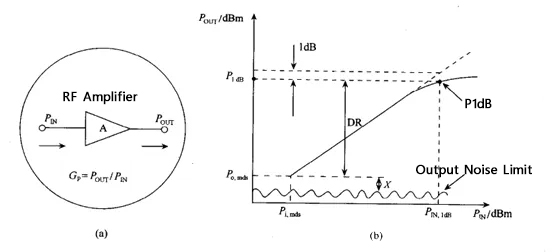
When the amplifier’s input power is relatively low, the power gain remains constant and the amplifier operates in the linear region. As the input power increases, the amplifier’s nonlinear characteristics gradually compress the power gain, which limits the maximum output power. If the power is increased further, the amplifier enters the saturation region, where its output power stays nearly unchanged. This behavior is illustrated in the figure below.
Hence P1dB = P0dB − 1 dB, where P0dB is the linear power under small-signal conditions.
Power Gain
Power gain is defined as output power minus input power. Under small-signal conditions, the power gain is relatively stable; under large-signal conditions, however, the power gain differs. For this reason, some amplifiers explicitly specify the gain at a particular output power level.
Operating Current
The operating current drawn by the amplifier when delivering a specified output power. Generally speaking, under the same conditions (e.g., the same linear power), the lower the current the better — lower current reduces heat dissipation and improves efficiency, which is one of the goals pursued in PA design today. Of course, these two parameters trade off against each other.
Efficiency
Power loss is inevitable in the conversion from input power to output power, and efficiency and linearity constrain each other. Common efficiency definitions for amplifiers are as follows:
- Collector efficiency = Pout / Pdc = Pout / (Udc × Idc)
- Power-added efficiency (PAE) = (Pout − Pin) / Pdc
- Total efficiency = Pout / (Pdc + Pin)
Harmonic Distortion
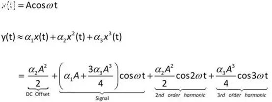
When a single-frequency signal is fed into the amplifier, the output contains not only the amplified fundamental signal but also its amplified harmonics, which may interfere with other frequency bands; therefore, the lower the harmonics, the better. This is normally tested, and the 3GPP specifications set explicit limits.
Intermodulation Distortion
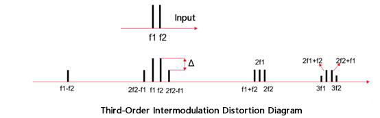
When the amplifier is driven by two signals at frequencies fc + fm and fc − fm (fc >> fm), the output contains, in addition to the harmonics of each signal, intermodulation distortion products generated by the sum and difference (intermodulation) of the input frequencies. The damage to the system is mainly caused by the odd-order intermodulation products (3rd, 5th, etc.) near the carrier frequency fc. Because these intermodulation products are extremely close to the carrier fc, they are difficult to eliminate with filters and readily interfere with adjacent frequencies. In practice, circuits use third-order intermodulation distortion to judge linearity.
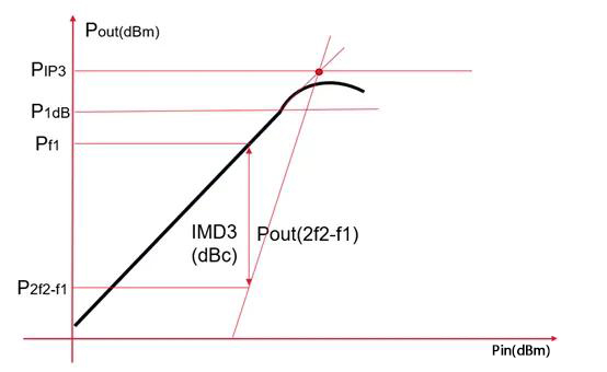
As shown in Figure 1, the third-order intermodulation products 2f1 − f2 and 2f2 − f1 are extremely close to the fundamental frequencies f1 and f2 and cannot be removed by filtering. In this case, IMD3 (third-order intermodulation distortion) is Δ = Pf1 − P(2f2−f1) (dBc).
Third-Order Intercept Point
As shown in Figure 2, the third-order intercept point (IP3) is the intersection of the extrapolated lines of the fundamental signal power and the third-order intermodulation product power. The relationships are:
OIP3 (dBm) = P1dB + 10.6 dB = Pf1 (dBm) + ½Δ = IIP3 + G
IIP3 = Pin + ½Δ
Δ = IMD3
ACPR
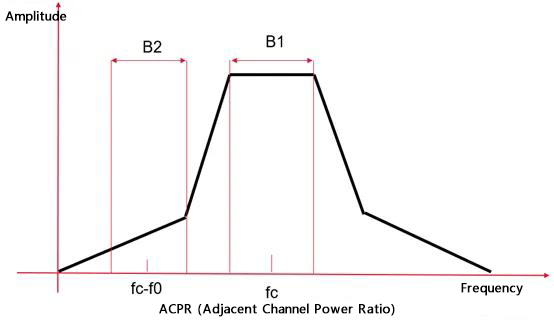
Due to the nonlinear effects of the power amplifier, a signal passing through it undergoes spectral “regrowth” (spreading). ACPR is defined as the ratio of the power in a bandwidth B1 centered at fc to the power in a bandwidth B2 offset from the center frequency f0, as shown in the figure below.
Tx Noise in Rx Bands
The various noise generated by the PA transmitter leaks into the receiver and causes demodulation interference in the receiver; generally, the smaller this value, the better.
Load Pull
When a power device operates at small signal, the input and output terminations are designed for the optimum conjugate matching. As the device enters the nonlinear region, conjugate matching at the input/output gradually no longer holds. To achieve maximum output power, load pull can be used to find the optimum load impedance ZL that yields the maximum output power of the power amplifier.
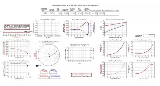
Load pull is the most accurate method for determining the optimum load impedance; it is used to simulate and measure the large-signal characteristics of the power transistor, such as output power, transducer power gain, two-tone intermodulation analysis, and so on. The input matching network is designed to provide sufficiently high gain, while the output matching network is designed to achieve the required output power.