Newsroom
PIN Diode Switch: How Much Do You Know about This?
The need for switching radio frequency (RF) signals at tens of GHz is pervasive and growing; currently, there are four basic switching technologies – electromechanical, PIN diode, analog, and MEMS – each with distinct characteristics and functions.
RF signal switching has been an essential function in design since the inception of wireless technology. This switching may be used internally within circuits for routing signals, sending (and receiving) signals to one of multiple antennas, or for testing matrices.
In this article, we will primarily discuss the main technologies, key properties, and main characteristics of PIN diode switching.
What is a PIN Diode Switch?
“PIN” is an abbreviation for “Positive – Intrinsic – Negative”. A PIN diode is a special type of diode, including PIN photodiodes and PIN switching diodes, which can be configured as radio frequency (RF) switches. It has a wide, undoped intrinsic semiconductor region (“I”) sandwiched between a p-type semiconductor region (“P”) and an n-type semiconductor region (“N”), hence the name PIN.
This differs from standard diodes, which lack an intrinsic region. Because of this intrinsic layer, PIN diodes have a wide range of applications, from low to high frequencies, primarily in the RF field, used as RF switches and RF protection circuits, and also as photodiodes.
PIN diodes possess excellent characteristics such as fast switching speed, high reverse breakdown voltage, high controllable power, low loss, and near-short-circuit and open-circuit properties under both forward and reverse biases. They are widely used in RF and microwave circuit design and have become an indispensable key component in electronic equipment used in military and civilian fields.
PIN diodes have excellent characteristics such as fast switching speed, high reverse breakdown voltage, high controllable power, low loss, and the ability to achieve near short circuit and open circuit under forward and reverse bias. They are widely used in the field of radio frequency and microwave circuit design, and have become one of the indispensable key components in electronic equipment in military and civilian fields.
How Does a PIN Diode Switch Work? the Principle
The working principle of a PIN diode can be simply described as follows:
- Structure: A PIN diode consists of three layers: a P-type semiconductor, an intrinsic semiconductor, and an N-type semiconductor. The intrinsic semiconductor layer is a lightly doped semiconductor, so free carriers are negligible.
- Forward Bias: When the PIN diode is forward biased, i.e., the P-terminal is connected to a positive voltage and the N-terminal to a negative voltage, current begins to flow. In this case, the current flowing from the P-terminal to the N-terminal is mainly composed of carriers (holes and electrons).
- Reverse Bias: When the PIN diode is reverse biased, i.e., the P-terminal is connected to a negative voltage and the N-terminal to a positive voltage, a reverse electric field is formed. Due to the presence of the intrinsic layer, this layer is relatively wide, meaning that electrons and holes need to overcome a large space charge region to move within the intrinsic layer under reverse bias.
- Low Leakage Current: Due to the presence of the intrinsic layer, electrons and holes need to traverse a wider intrinsic region under reverse bias, which increases the resistance of the leakage current. Therefore, the reverse leakage current of PIN diodes is relatively low.
- Higher reverse breakdown voltage: Due to the width of the intrinsic layer, the reverse breakdown voltage of PIN diodes is relatively high. Reverse breakdown voltage refers to the voltage at which a diode breaks down when the reverse voltage exceeds a certain threshold.
What is a PIN Diode Switch Used for? the Applications
PIN diodes, due to their unique characteristics, are used in many electronic circuits, primarily including:
As high-voltage rectifiers
PIN diodes are used as high-voltage rectifiers. The wide intrinsic layer gives the diode the ability to withstand high reverse voltages without breakdown. Therefore, high-voltage rectification can be achieved using PIN diodes.
As radio frequency (RF) switches
PIN diodes can be used as RF and microwave switches, but in this case, the diode needs to operate in the reverse bias region. A wider intrinsic layer results in a smaller junction capacitance.
In RF PIN switches, when the PIN diode is in the on state, the RF signal can pass through the type I region, closing the switch; when the PIN diode is in the off state, the depletion layer of the type I region impedes the passage of the RF signal, opening the switch.
As photodiodes
PIN diodes can also be used as photodiodes. The conversion of current to light occurs in the intrinsic region of the diode. Therefore, the wider the intrinsic region, the higher the efficiency of light generation by the diode.
As attenuators and RF protection circuits
When forward biased, a PIN diode acts as a variable resistor. Therefore, it can be used to protect RF circuits from large currents that could damage the circuit. When the forward bias voltage increases, the resistance suddenly decreases, so it can be used as an attenuator.
Under Which Condition Does a PiN Diode Act as a Switch?
PIN diodes function as traditional diode rectifiers at low frequencies. However, at microwave frequencies, their IV curve changes, and they act as current-controlled resistors, with their resistance value determined by the magnitude of the DC current.
Therefore, a PIN diode is a DC-controlled high-frequency resistor; without DC current, the diode functions like an open circuit.
What is the Frequency Range of a PIN Diode Used as an RF Switch?
This mainly depends on the thickness of the I-region; thicker diodes can operate below 1 MHz, while thinner diodes can operate below several GHz. It’s important to note that, unlike electromechanical RF switches, PIN diodes cannot operate at DC.
How Does Temperature Affect PIN Diodes?
The effect of temperature on PIN diodes is complex and needs to be considered comprehensively based on specific operating conditions. It mainly manifests in the following aspects:
1. Forward Voltage Drop (VF)
- At low current: As temperature increases, the intrinsic carrier concentration increases, the junction voltage decreases, and VF exhibits a negative temperature coefficient.
- At high current: As temperature increases, carrier mobility decreases, resistance increases, and VF increases with increasing temperature, exhibiting a positive temperature coefficient.
2. Reverse Leakage Current (IR)
As temperature increases, minority carrier injection is enhanced, and leakage current increases significantly.
3. Reverse Recovery Characteristics
As temperature increases, minority carrier lifetime lengthens, the reverse recovery time (TRR) becomes longer, the recovery process is slower, and it may lead to higher reverse recovery losses.
4. Breakdown Voltage (BV)
With a small increase in temperature, carrier scattering is enhanced, and the breakdown voltage (BV) increases slightly, but it may decrease after exceeding a certain temperature.
5. Resistance (R)
The temperature-resistance characteristic of microwave PIN diodes depends on the combined effects of carrier lifetime and mobility. A diode with a small junction capacitance has a small change in resistance with temperature; a diode with a large junction capacitance may have a linear increase in resistance with increasing temperature.
What are the Challenges of Designing Using PIN Diodes?
The biggest challenge lies in its dual-terminal nature; therefore, the control signal (DC bias) and the RF signal share the same terminals. This means they must be combined before entering the diode and then separated.
This requires a circuit topology that uses inductors and capacitors to separate the signals, and the values of these inductors and capacitors are difficult to determine because they are functions of frequency, bandwidth, diode characteristics, layout parasitic parameters, etc.
Therefore, many suppliers offer complete modules of PIN diode RF switches, which include all the supporting circuitry, greatly simplifying this challenge. You can contact our experts for an inquiry.
What are the Advantages and Disadvantages of PIN Diodes?
The Advantages of PIN Diodes
- Small Capacitance, High Frequency: The presence of the intrinsic layer allows the depletion region to expand without an external voltage, and the depletion layer width of the PIN diode can be wider, which is highly beneficial for reducing capacitance and increasing switching speed. Due to the wider depletion region, PIN diodes exhibit better performance in high-frequency applications, making them suitable for RF and microwave applications.
- Lower Forward Voltage Drop: Under forward bias, the voltage drop of a PIN diode is typically lower than that of a conventional PN junction diode due to the conductivity modulation effect, which helps improve overall circuit efficiency.
- Lower Reverse-bias Leakage Current: Due to the lower doping concentration of the intrinsic layer and the thicker I-region, the thickness and doping level of the I-region affect the reverse leakage current of the PIN diode. By appropriately selecting the thickness and doping level of the I-region, the leakage current can be reduced.
- High Linearity: The intrinsic layer has a much wider depletion region than that of a conventional PN junction diode. Under reverse bias, this wide depletion region provides higher resistance, which helps improve linearity and reduce signal distortion. Under forward bias, the current and voltage in the PIN diode are linearly related. This characteristic is crucial for maintaining signal linearity, especially in analog signal processing.
- Low Noise: The lower carrier concentration in the intrinsic layer means less carrier recombination and generation during signal processing. This lower carrier activity helps reduce noise, particularly low-frequency noise. PIN diodes generate lower noise during signal amplification and, due to their wide depletion region, exhibit better electromagnetic compatibility in high-frequency applications, thus reducing noise caused by electromagnetic interference.
- High Voltage Breakdown: The lightly doped region of the intrinsic layer enhances the diode’s voltage breakdown capability, allowing it to withstand higher reverse voltages.
- Superior Thermal Stability: The intrinsic layer of a PIN diode provides a physical barrier, reducing diffusion and impurity migration that can occur between the P-type and N-type regions at high temperatures, resulting in better thermal stability.
- Photoelectric Reaction: Due to the wider intrinsic layer, more photons impact the surface, and the generation of electron-hole pairs increases. This leads to greater current flow. Therefore, PIN diodes contribute to improved photoelectric detection.
The Disadvantages of PIN Diodes
-
- Slower Switching Speed
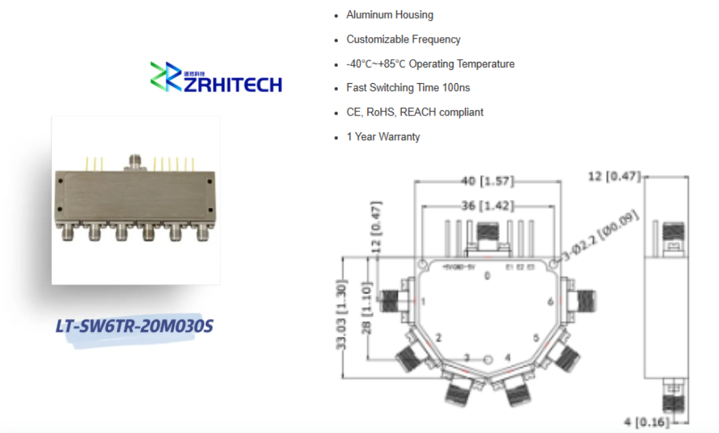
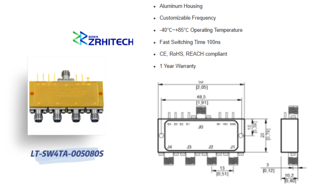
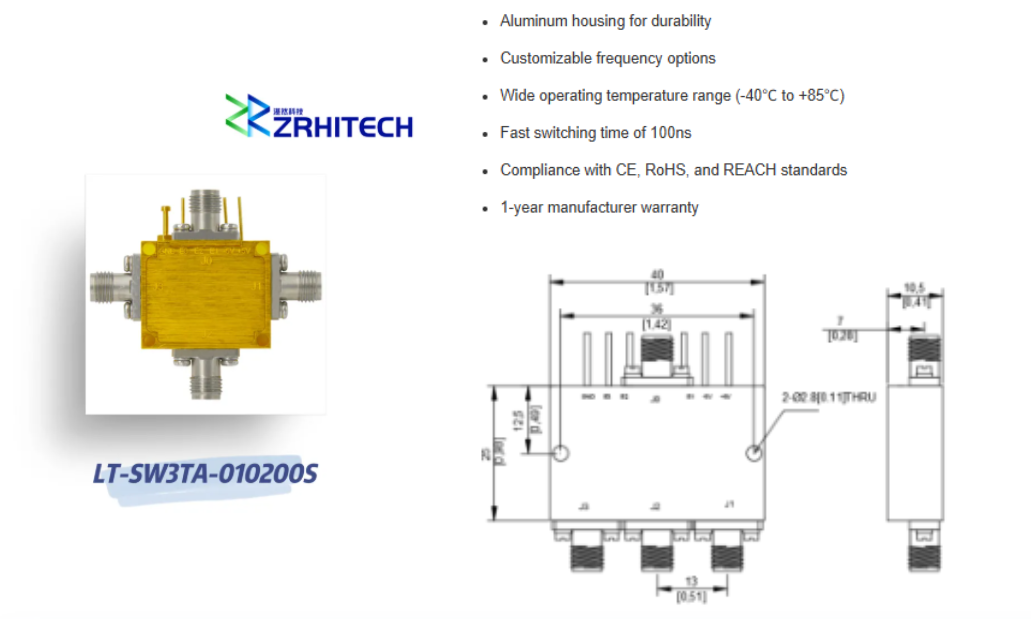
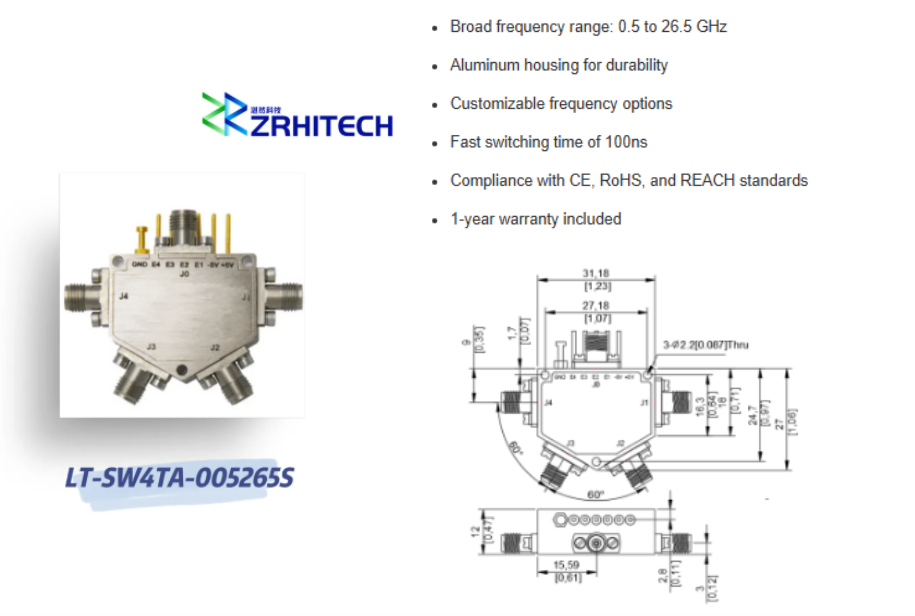 0.5 To 26.5 GHz SP4T Absorptive PIN Diode Switch
About ZR Hi-Tech: Leading PIN Diode Switch Manufacturer
ZR Hi-Tech is a company specializing in integrated circuit manufacturing, committed to providing customers with high-performance, high-reliability integrated circuit solutions. Our team consists of experienced professionals.
If you are looking for a reliable PIN diode switch manufacturer solution for your project, please consult with ZR Hi-Tech experts!

ZR Hi-Tech’s Product Advantages and Core Capabilities
With deep technological expertise, we have built a comprehensive product portfolio of PIN diode switches, dedicated to providing professional solutions for our customers.
High Reliability Assurance: Our PIN diode switch product line adheres to stringent quality standards, undergoes comprehensive environmental stress screening and reliability testing, and complies with CE, RoHS, and REACH standards.
Deep Customization Services: We possess strong custom development capabilities and can provide flexible customization services based on specific customer needs. For customized specifications or special requirements, please contact us directly.
- : While performing well in high-frequency applications, PIN diodes typically have slower switching speeds than other types of diodes, such as Schottky diodes. Their poorer reverse recovery characteristics significantly impact switching losses.
- Increased Complexity and Cost: Manufacturing PIN diodes is relatively complex, potentially leading to increased costs.
- Reduced Carrier Injection Efficiency: The intrinsic layer can reduce carrier injection efficiency from the P-type and N-type regions to each other, which can affect the performance of certain types of circuits.