Newsroom
RF Amplifier Chip Classification, Applications, and Selection Guide
In wireless communication, radar, and drone RF systems, RF amplifiers play an important role. Their main job is to boost RF signal power. Different applications have different technical requirements. As a result, RF amplifiers come in various types and configurations. This article briefly explores the common categories of RF amplifier chips, their applications, and key factors to consider when selecting them.
RF Amplifier Types and Applications
According to the common classifications based on the application scenarios of amplifiers:
- LNA, or Low Noise Amplifier
An LNA is mainly used to amplify weak signals while adding as little noise as possible. This helps improve the signal-to-noise ratio (SNR). In a signal chain, the overall noise figure is strongly influenced by the early stages. Therefore, LNAs are often placed at the front end of a receiver. This helps maximize receiver sensitivity.
- DPA,Drive Amplifier
The core role of a medium-power driver amplifier is to optimize the operating conditions of connected devices. This helps ensure that they work at their best. It provides a strong enough drive signal for the following devices. These may include a second amplifier, mixer, converter, and other components.
- GB,Gain Block Amplifier
Gain block amplifiers focus on providing good gain flatness and return loss. Their design usually includes internal matching and bias circuits.
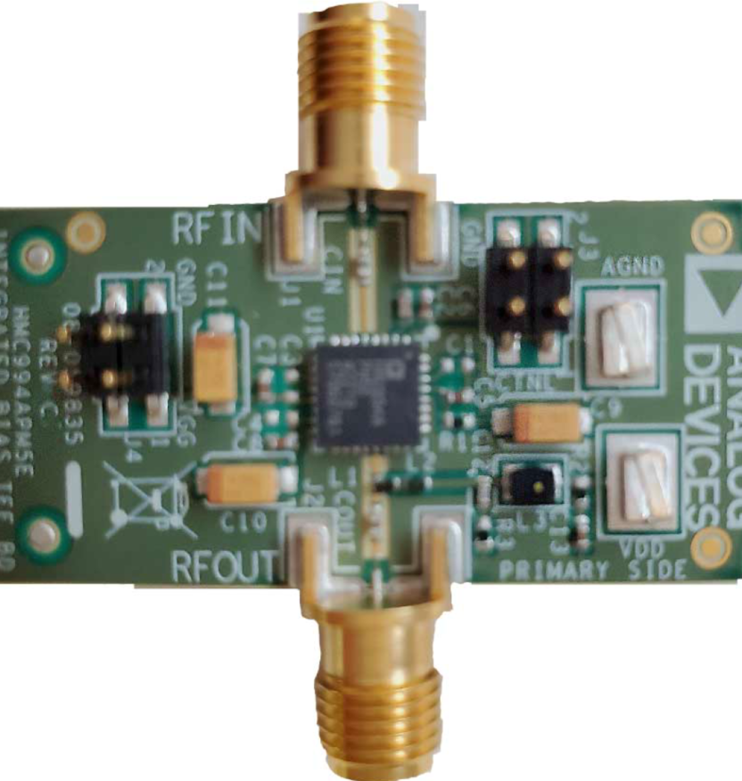
RF amplifiers are mainly divided into four categories: low‑noise amplifiers, high‑power amplifiers, driver amplifiers, and gain‑block amplifiers.
- Low‑noise amplifiers feature high gain and low noise figure. They are primarily deployed in receive channels to improve receiving sensitivity.
- High‑power amplifiers deliver high output power with high P‑1dB and saturated power. They serve as the final‑stage amplification in transmit channels to boost transmit power.
- Driver amplifiers are medium‑power amplifiers placed before the PA. They raise the input signal power of the subsequent PA to achieve target high output power. They can also act as the final‑stage amplifier for medium‑power transmit channels.
- Gain‑block amplifiers provide good gain flatness and return loss, with integrated matching and bias circuits inside.
Based on different semiconductor material processes:
GaAs Power Amplifier
- GaAs (Gallium Arsenide) power amplifiers are widely used because of their excellent RF performance.
GaN Power Amplifier
- GaN (gallium nitride) power amplifiers are a new type of amplifier that has emerged with the rise of third-generation semiconductor materials. GaN power amplifiers have higher power density and better operating efficiency, making them perform exceptionally well in high-power, high-frequency applications.
RF Amplifier Chip Performance Specs
When choosing and evaluating the performance of RF/microwave amplifier chips, the key indicators are gain, gain flatness, P-1dB compression point, saturated power, output IP3, input return loss, and output return loss. These parameters directly determine the amplifier’s compatibility in the signal chain, signal fidelity, and system stability. Here’s what each of these indicators means:
Frequency
RF amplifiers generally cover frequencies up to 50GHz, such as 0.5–6GHz, 0.8–18GHz, and 18–40GHz.
Gain
The gain of an amplifier refers to the ratio of the output signal power (or voltage) to the input signal power (or voltage), usually measured in decibels (dB). In the RF field, power gain is commonly used: G(dB) = 10lg(Pout/Pin). Gain is the most basic metric of an amplifier, showing how well it can boost a signal.
Gain Flatness
Gain flatness refers to the maximum variation in an amplifier’s gain within a specified frequency range, measured in dB. For example, if an amplifier has a gain of 20±0.5 dB in the 1–6 GHz range, then the flatness is ±0.5 dB.
P-1dB Compression Point
The output P-1dB compression point is the output power level where the amplifier’s output power deviates by 1 dB from the linear increase with input power. It’s a key measure of the upper limit of an amplifier’s linear operating range and shows the maximum output capability before noticeable distortion occurs.
Psat,Saturated Output Power
When the input power keeps increasing but the amplifier’s output power stops rising with it, the output power at that point is called the saturated output power. At this stage, the amplifier’s gain drops to about half of its linear gain (a 3 dB drop). This reflects the amplifier’s maximum output capability and is a key indicator for power amplifiers. When working in the saturation region, the signal distortion is very high, and harmonic components and intermodulation products increase significantly, so it’s only suitable for situations where distortion doesn’t matter.
Third-Order Intercept Point
IP3 (third-order intercept point) is a virtual metric for measuring an amplifier’s linearity. When you input two sine waves with close frequencies, f1 and f2, the amplifier’s nonlinearity produces intermodulation products. Among these, the third-order products 2f1−f2 and 2f2−f1 can fall within the signal bandwidth and interfere with the desired signal. IP3 is the virtual output power point where the third-order intermodulation product power equals the fundamental power, measured in dBm. IP3 is the key standard for amplifier linearity—the higher the IP3, the better the linearity and the lower the intermodulation distortion.
Return Loss
Return loss reflects how well the amplifier port matches the impedance of the circuits before and after it. The standard impedance in RF systems is 50 ohms, and a good impedance match can reduce signal reflections.
RF Amplifier Chip Power Supply
RF amplifier chips require a DC power supply with minimal ripple. Low‑noise LNAs typically adopt a single positive supply. Its voltage is below 8 V, and 5 V is the most common value. The operating current is generally less than 80 mA. Medium‑ and high‑power amplifiers usually use dual positive‑negative power supplies. The positive drain voltage VDD is commonly 5‑12 V.
The negative gate voltage VGG typically ranges from ‑1 V to ‑0.2 V. Important note: VGG must be powered up before VDD. Failure to follow this sequence may damage the chip. Their operating current falls between 100 mA and 800 mA. During circuit design and debugging, adjust VGG to achieve the rated operating current. Some amplifier chips have no dedicated power pin. They receive power via the bias circuit at the RF output port. Inductor and capacitor values for this bias circuit must strictly follow the chip manufacturer’s reference schematic.
Conclusion
RF amplifiers are fundamental building blocks for wireless communication, radar, and drone RF systems. Different types including LNAs, driver amplifiers, gain‑block amplifiers and high‑power amplifiers serve distinct positions within the signal chain. Low‑noise amplifiers optimize receiver sensitivity at the front‑end, while driver and high‑power amplifiers deliver sufficient signal power for transmit paths. Material technologies such as GaAs and GaN further expand design options for different power‑frequency requirements.
When selecting an RF amplifier chip, engineers need to evaluate a full set of key specifications. Frequency range, gain, gain flatness, P‑1dB, saturated output power and output IP3 define amplification capability and linear performance. Return loss determines impedance matching quality for stable system integration. Besides performance parameters, power‑supply rules also deserve close attention. Proper DC supply ripple, correct power‑on sequence for high‑power devices, and compliance with recommended bias‑circuit components are critical to avoid chip damage during practical circuit implementation.
Choosing the right amplifier is not only about picking high‑specification components. It requires matching device characteristics to real‑world system demands, balancing gain, linearity, output power and power‑supply constraints. If you are looking for reliable RF amplifier solutions for your projects, contact ZR Hi‑tech for professional technical support and customized device options to meet your system design goals.