Newsroom
From Low Noise to High Power: Advancing Low Noise Amplifier Performance for 5G, Satellite, and High-...
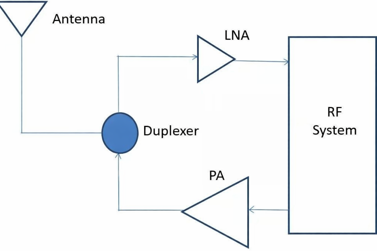
The demands for performance, miniaturization, and higher frequencies are challenging the limitations of two key antenna connection components in wireless systems: power amplifiers (PAs) and low noise amplifiers (LNAs). The development of 5G and the use of PAs and LNAs in microwave radio links, VSAT (satellite communication systems), and phased-array radar systems are driving this shift. These applications require lower noise (for LNAs), higher energy efficiency (for PAs), and operation at frequencies up to or above 10 GHz. To meet these growing demands, LNA and PA manufacturers are shifting from traditional all-silicon processes to gallium arsenide (GaAs) for LNAs and gallium nitride (GaN) for PAs. This article will introduce the roles and requirements of LNAs and PAs and their key characteristics, followed by a discussion of typical GaAs and GaN devices and design considerations when using these devices.
Sensitivity of Low Noise Amplifier
The function of an Low Noise Amplifier is to capture extremely weak and uncertain signals from an antenna. These signals are typically at the microvolt level or below -100 dBm. The LNA then amplifies them to a more useful level, usually around 0.5 to 1 V .In a 50 Ω system, 10 μV corresponds to -87 dBm, while 100 μV equals -67 dBm. Although such gain can be achieved with modern electronics, the challenge lies in noise. When noise is introduced into these weak input signals, the situation becomes much more complex. In fact, excessive noise can completely negate the amplification advantage of the LNA.
LNAs operate in a highly uncertain environment. As the front end of a transceiver, an LNA must capture and amplify very low-voltage signals. These signals exist within a defined bandwidth and are often mixed with random noise from the antenna. At the same time, the LNA must maintain extremely low power consumption. In signal theory, this scenario is known as the “unknown signal/unknown noise” problem. It is considered one of the most challenging issues in signal processing. The key parameters of an LNA include noise figure (NF), gain, and linearity.
Noise mainly originates from thermal effects and other internal or external sources. The typical noise figure of an LNA ranges from 0.5 to 1.5 dB. A single-stage amplifier usually provides a gain of 10 to 20 dB. Some designs use cascaded stages. In these designs, a low-gain, low-noise stage is placed first, followed by a higher-gain stage. This approach may increase the overall noise figure. However, once the initial signal has been amplified, the impact of additional noise becomes less significant.
Another important issue in LNAs is nonlinearity. Nonlinearity can generate harmonics and intermodulation distortion. These unwanted signals degrade the quality of the received signal. As a result, demodulation and decoding become more difficult, especially when a low bit error rate (BER) is required. The third-order intermodulation point (IP3) is commonly used to evaluate linearity. It measures the relationship between nonlinear distortion products and the desired linear signal. A higher IP3 value indicates better linearity and overall amplifier performance.
Power consumption and energy efficiency are generally not primary concerns for LNAs. Most LNAs naturally operate with low power consumption. Their current draw typically ranges from 10 to 100 mA. They provide voltage gain to the next stage, but they do not deliver power to the load. In most systems, only one or two LNAs are used. In some cases, two LNAs are applied in multi-functional antenna designs, such as Wi-Fi and 5G systems. Because of this limited usage, reducing power consumption in LNAs does not significantly impact overall system energy efficiency.
Aside from operating frequency and bandwidth, various LNAs are relatively similar in function. Some LNAs also have gain control, thus enabling them to handle a wide dynamic range of input signals without overload or saturation. Such a wide range of input signal strength variation is frequently encountered in mobile applications with wide base station-to-mobile channel losses, even in single-connection loops.
Low Noise Amplifier Layout, Impedance Matching, and GaAs Device Implementation Considerations
The routing of input and output signals in an Low Noise Amplifier is just as important as the component specifications. Designers must use advanced modeling and placement tools to achieve optimal performance. Even high-quality components can suffer from poor layout or improper impedance matching. These issues can significantly degrade overall performance. Therefore, it is essential to use the Smith chart provided by the vendor. A reliable circuit model that supports simulation and analysis is also critical.
For these reasons, most high-performance Low Noise Amplifier vendors operating in the GHz range provide evaluation boards or proven PCB layouts. Every aspect of the test setup is critical. This includes layout, connectors, grounding, bypassing, and power supply design. Without these resources, it is difficult to achieve accurate performance results. Designers would otherwise spend significant time evaluating components in real applications.
Examples
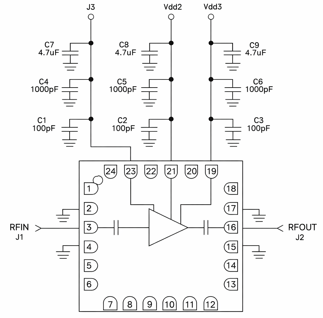
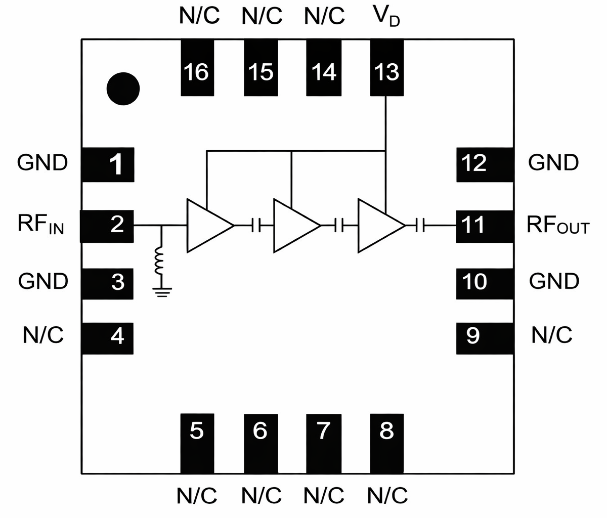
A representative GaAs-based LNA is the HMC519LC4TR. This is an 18 to 31 GHz pHEMT (pseudocrystalline high electron mobility transistor) device from Analog Devices. This leadless 4×4 mm ceramic surface-mount package offers 14 dB of small-signal gain, a low noise figure of 3.5 dB, and a high IP3 of +23 dBm. The device can draw 75 mA of current from a single +3 V supply.
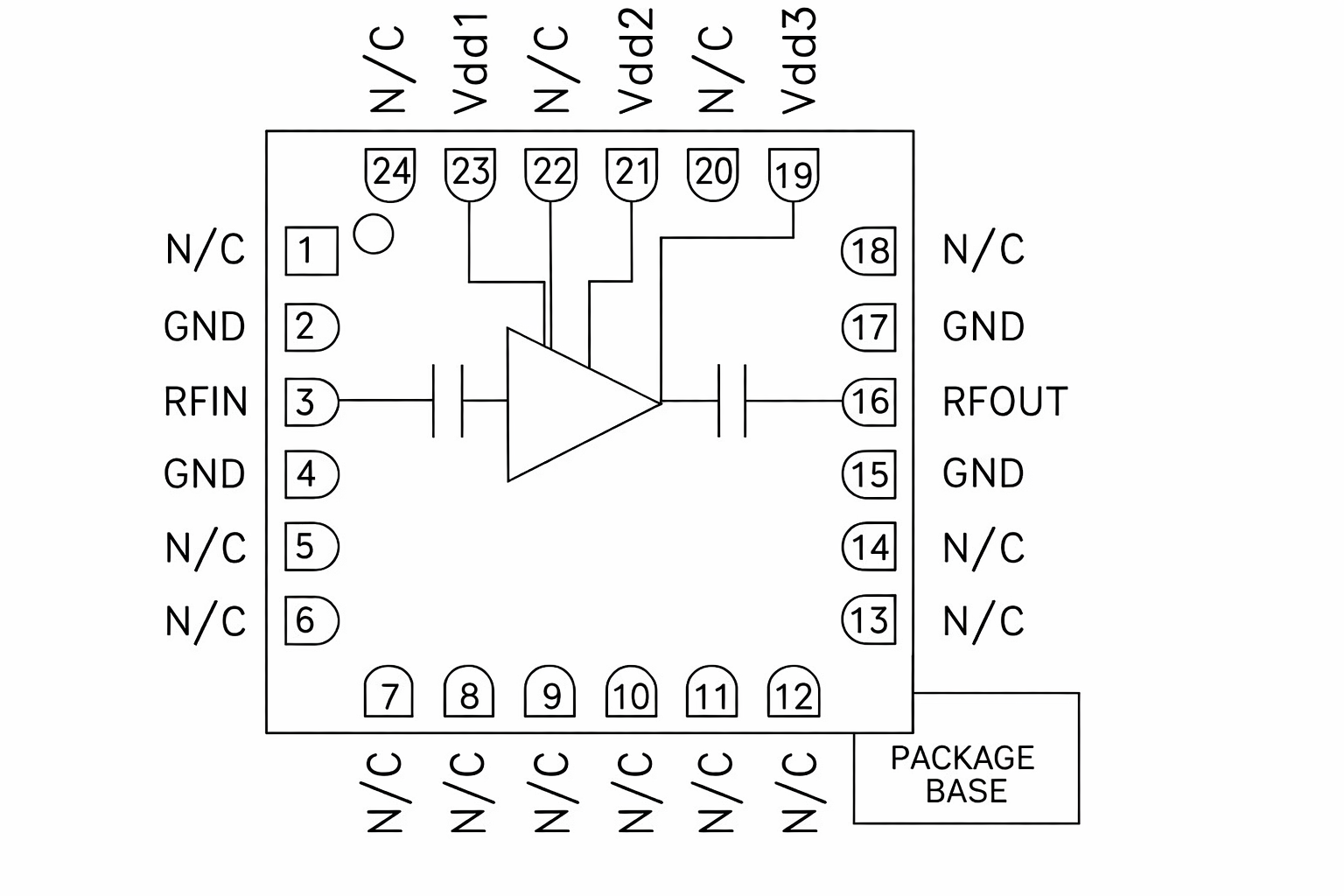
From a simple functional block diagram to multiple external capacitors with different values and types, a design process is required, providing appropriate RF bypass, low parasitic effects on three power rail feeds, and specified as Vdd.
The MACOM MAAL-011111 is a GaAs LNA for higher frequencies, supporting operation from 22 to 38 GHz. This device offers a small-signal gain of 19 dB and a noise figure of 2.5 dB. While superficially a single-stage device, this LNA actually contains three cascaded stages internally. The first stage is optimized for minimum noise and moderate gain, while subsequent stages provide additional gain.
Similar to Analog Devices’ LNAs, the MAAL-011111 requires only a low-voltage supply and is extremely compact, measuring only 3×3 mm. Users can adjust and trade off certain performance specifications by setting the bias (supply) voltage between 3.0 and 3.6 V. The recommended board layout shows the key printed circuit board copper dimensions required to maintain proper impedance matching and ground plane performance.
Conclusion
The evolution of 5G, satellite communication, and high-frequency RF systems is placing increasingly stringent demands on both low-noise amplifiers (LNAs) and power amplifiers (PAs). As systems push toward higher frequencies, lower noise, and greater efficiency, the shift to advanced semiconductor technologies such as GaAs for LNAs and GaN for PAs has become essential.
For LNAs in particular, achieving optimal performance requires careful balancing of noise figure, gain, and linearity, along with precise attention to PCB layout, impedance matching, and system integration. Even the highest-quality components can underperform without proper design and implementation.
By understanding these key principles and leveraging proven device technologies, engineers and B2B buyers can build more reliable, high-performance RF front-end systems. As a trusted manufacturer, ZR Hi-Tech is committed to delivering innovative RF solutions that meet the evolving needs of modern wireless applications. Contact us today to explore how our LNA and PA solutions can enhance your next-generation RF systems.