Newsroom
Basics of Low Noise Amplifier Design: Key Parameters & Practical Design Tips
The wireless communication industry keeps evolving. Greater focus is being placed on the performance of RF front‑end solutions. Modern wireless systems include 5G base stations, satellite communications, radar and spectrum‑monitoring equipment. They demand higher receiver sensitivity under complex signal environments. The low noise amplifier (LNA) is the first active component inside a receiver.
It strongly influences overall receiver‑system performance. It is placed right after the receiving antenna. It amplifies extremely weak incoming RF signals with minimal additional noise. Noise introduced by the LNA travels through the following circuit chain and cannot be easily removed by later‑stage blocks. Thus, well‑optimized LNA design lays a solid foundation for high‑sensitivity RF receivers.
Basic Theory of Noise
The performance and noise of an LNA are closely related, and it’s mainly because the components inside the LNA are easily affected by noise.
In communication RF circuits, the usual sources of noise are mainly divided into the following types:
Thermal Noise
The introduction of thermal noise is usually the result of the Brownian motion of charges in a conductor, and this motion increases as the temperature rises, with the random movement of charges causing random voltage.
This kind of noise process is random, so in physics it’s usually described using statistical methods. The mean square noise voltage of thermal noise can be described by the following formula:
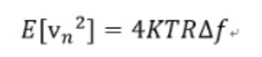
You can use the equivalent Thevenin theorem to model thermal noise equivalently as shown in the diagram below, which is just a noiseless resistor in series with a noise voltage source with a mean square value of  .
.
Because there are a huge number of electrons in a conductor and their random movements are statistically independent of each other, according to the central limit theorem, thermal noise follows a zero-mean Gaussian distribution.
Shot Noise
The fundamental reason for shot noise is that electric charge has particle-like properties.
To make shotgun noise, you need to meet these two conditions:
1.There has to be a direct current flowing;
2.There has to be a potential barrier that charge carriers can jump over, so commonly used linear resistors don’t really produce shot noise.
The discrete nature of charges causes discontinuous current pulses whenever an electron jumps over an energy barrier. It’s exactly the randomness in the arrival times of electrons that leads to the full-spectrum characteristic of shot noise (white noise characteristic).
The RMS current of the shot noise can be expressed as:
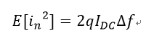
The need for a potential barrier means that shot noise is only linked to nonlinear devices, but not all nonlinear devices show it. In BJTs, because there are two PN junctions, both the base current and collector current can be noise sources. In FETs, though, only the gate-to-drain current can cause shot noise, but it’s really tiny, so it’s not a major noise source.
Flicker Noise
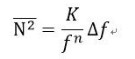
Flicker noise, also known as 1/f noise, is very common, but there isn’t a universally applicable mechanism for it. This type of noise is characterized by the noise power density spectrum decreasing as the frequency increases, and its empirical mathematical expression is:
Low Noise Amplifier Related Parameters
The low-noise amplifier (LNA) is located at the front end of the RF receiver and is the first active circuit of the receiver.
From the noise of a cascaded system. We know that the noise figure of the first stage directly adds to the total system noise figure. So the LNA’s noise figure needs to be designed as low as possible.
At the same time, to improve the receiver’s sensitivity, the LNA needs to provide enough gain.
Additionally, to minimize distortion during signal amplification, the LNA should have good linearity.
Also, there is usually a passive filter (typically SAW or BAW) between the LNA and the antenna for filtering. And the filter’s performance is very sensitive to its load impedance.
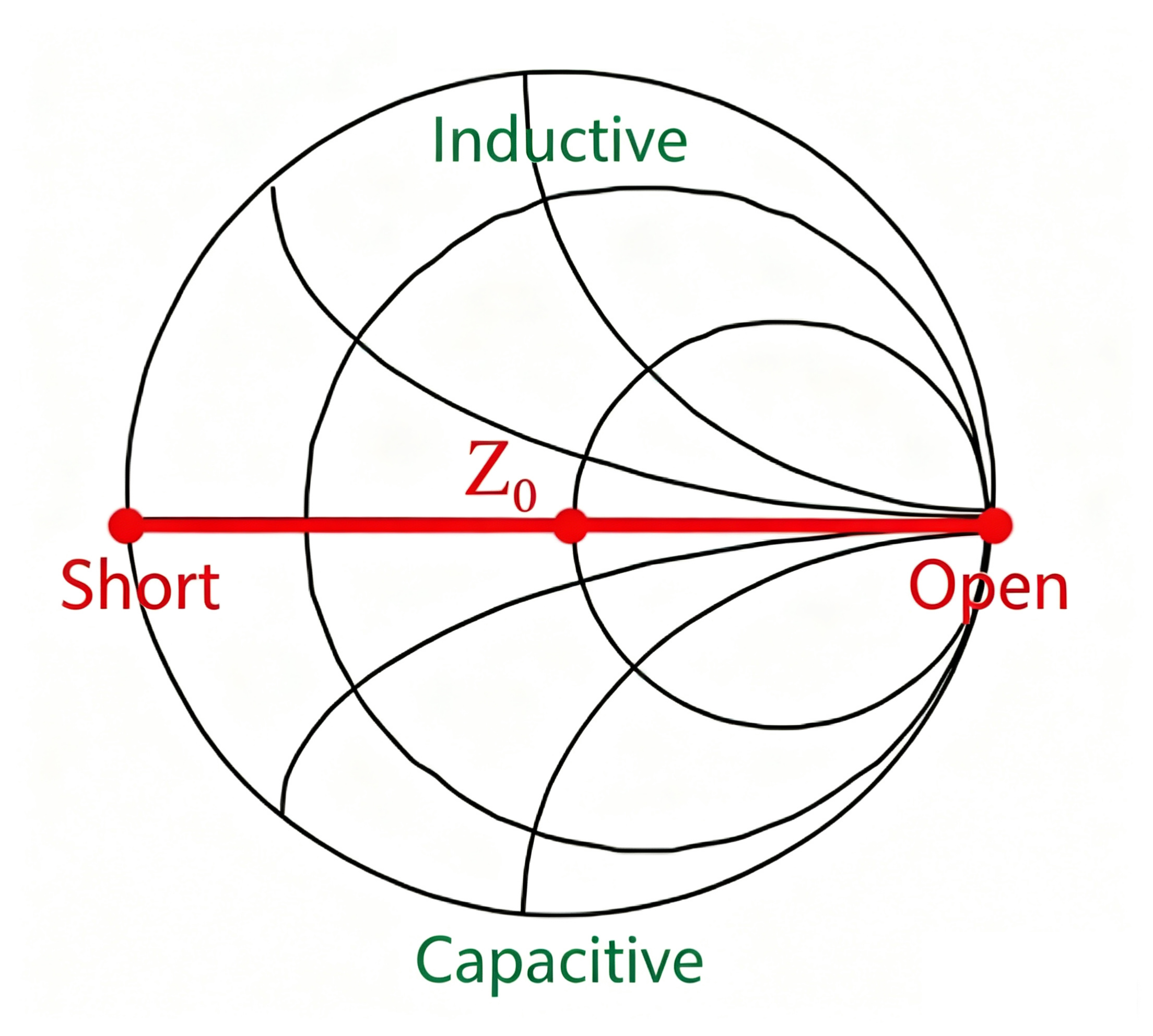
So, to get good filtering characteristics, the LNA’s input impedance should match the output impedance of the front-end filter, which is usually 50 ohms.
The Z0 position on the Smith chart is shown below:
Noise Figure
Noise figure is usually used to measure the amount of internal noise in a circuit or system, and it’s often used to compare the noise performance of different circuits or systems.
The definition of noise figure is as follows:
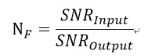
Since the amplifier itself has noise, the signal-to-noise ratio at the output is different from that at the input. For this reason, the noise figure is used to measure the amplifier’s own noise level.
This coefficient represents how much the amplifier’s noise performance has worsened. It’s not the case that bigger is better. The larger its value, the more noise is added during transmission, reflecting the imperfections of the device or the channel.
Usually, the noise figure is related to temperature—the higher the temperature, the higher the noise figure.
Gain
Gain is an important parameter for low-noise amplifiers. If a low-noise amplifier has a relatively high gain, it can not only amplify signals but also effectively suppress noise from downstream circuit modules.
However, if the gain is too high, the linearity requirements for the downstream circuit modules increase; otherwise, signal saturation may occur, leading to signal distortion.
The typical gain for a single-stage LNA is usually between 10 and 20 dB.
Input-output Matching
In real RF systems, the front end of a low-noise amplifier (LNA) is usually a high-performance external pre-selection RF filter. Its output port is connected to the input of the LNA. To achieve maximum power transfer, the LNA’s input impedance needs to match 50Ω.
If the LNA’s input impedance deviates from 50Ω, causing an impedance mismatch, there are two consequences:
1. It can cause power reflection, which affects the amount of signal power received by the LNA;
2. It might worsen the performance of the front-end RF filter, thereby degrading the overall system performance.
Linearity
Friends who have studied analog circuits should be pretty familiar with transistor characteristics. The output characteristic curve of an amplifier will change depending on the transistor’s bias point, which comes from the inherent nonlinearity of the transistor.
We all hope that the amplifier is ideally linear, meaning that no matter how much input power there is, the output power increases linearly (with a constant gain).
But in reality, there’s no such thing as an ideally linear amplifier. As the input power increases, the output power might not increase linearly.
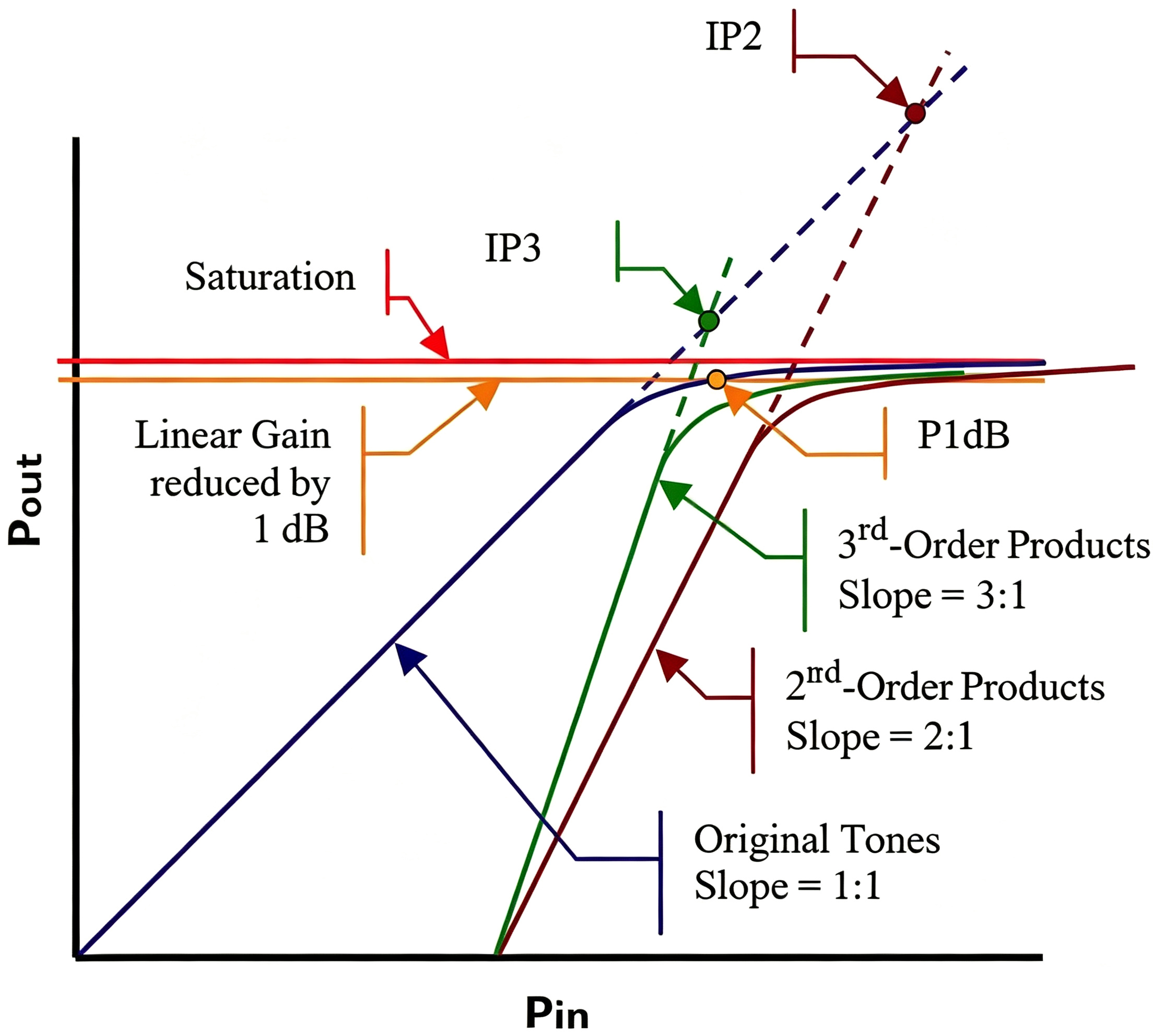
As shown in the figure below, when the input power is low, the gain is close to linear. As the input power keeps increasing, the output power roughly increases linearly at first. But after reaching a certain point, the nonlinearity becomes more obvious, leading to gain compression. The output power grows more slowly and eventually stabilizes near saturation. The relationship between the input and output power is shown in the figure below:
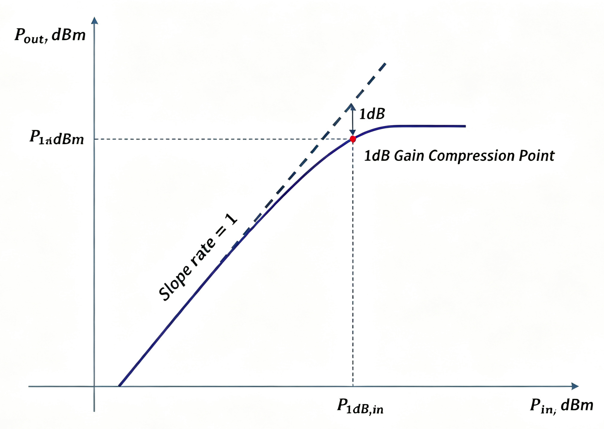
First of all, it’s important to clarify that this is a logarithmic representation of input and output power, so the ideal linear amplifier curve has a slope of 1, as shown by the dashed line in the figure.
The solid line represents the relationship between the actual input and output power of the amplifier. As the input power increases, the output power grows more slowly, gradually deviating from the ideal curve, and the gain drops step by step. This is what’s called gain compression.
Active devices like amplifiers usually pay attention to the point where the actual gain drops 1dB below the linear gain, called the 1dB gain compression point. The input and output powers at this point are generally labeled as P1dB,in and P1dB,out respectively.
The higher the 1dB gain compression point, the better. When comparing two amplifiers, the one with the higher compression point has better linearity.
Nonlinear Distortion
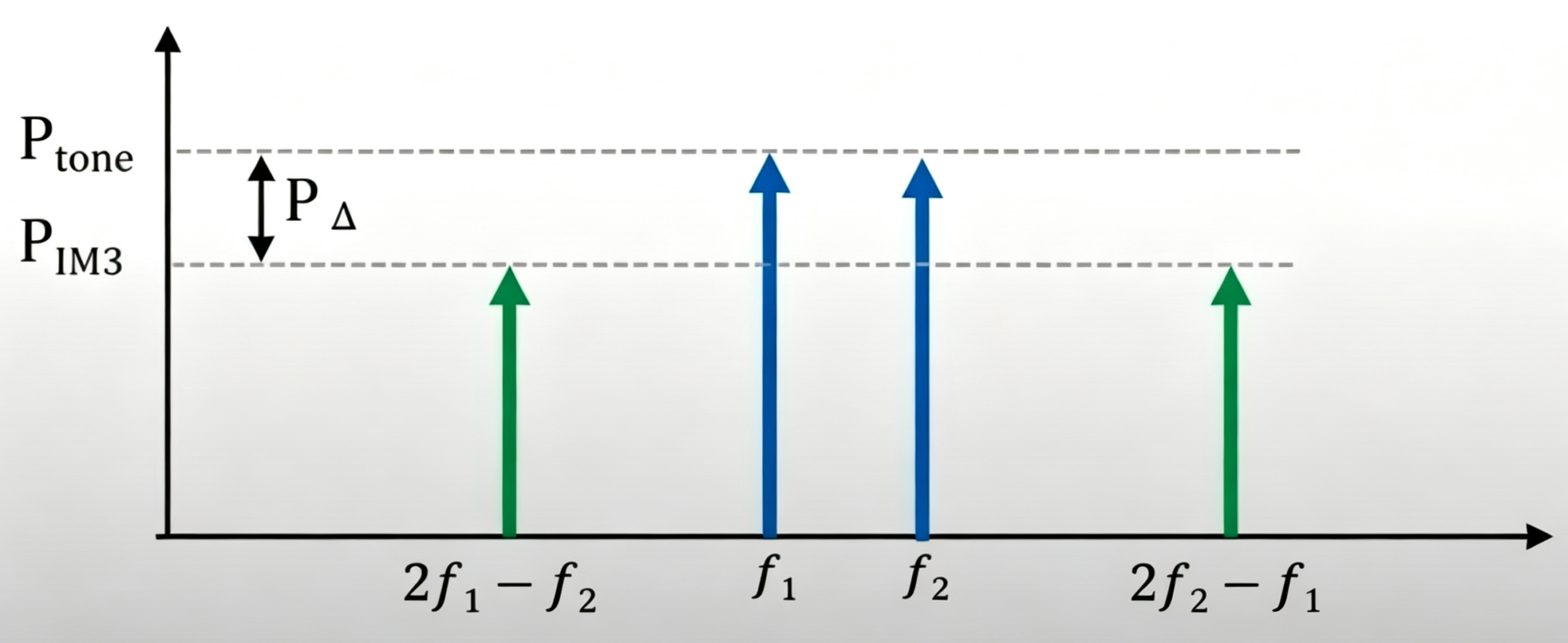
Signals in wireless communication systems have finite bandwidth. When total power gets close to the 1 dB compression point, the amplifier shows stronger nonlinear behavior. It generates obvious harmonics and intermodulation products, which can interfere with adjacent and in‑band channels.
So, nonlinear distortion is a really important thing to think about when designing amplifiers.
So the Pi (1dB) point is a really important parameter for measuring linearity.
Besides that, TOI (Third-order Intercept) / IP3 point is also an important parameter to measure linearity. It mainly indicates how the device’s harmonic and intermodulation signals affect linearity.
Reverse Isolation
Reverse isolation represents the performance of isolating the input and output ports of an LNA. Numerically, it’s defined as the attenuation of a signal traveling from the output port to the input port, usually expressed by the S-parameter S12.
The higher the signal attenuation from the output to the input, the better its unidirectional performance and reverse isolation. Good isolation can effectively prevent the local oscillator signal from leaking through the LNA from the mixer to the antenna, stopping strong LO signals from radiating into space and causing interference to other communication systems.
Moreover, good isolation also makes circuit design easier. It allows the LNA design to be almost unidirectional, so when designing the input matching circuit, you don’t need to worry about the output matching circuit’s effect, and vice versa.
The reverse isolation of an LNA is heavily influenced by the Miller effect and parasitic capacitance, so a cascode structure is usually used to improve its reverse isolation performance.
Conclusion
An LNA is a critical RF‑receiver front‑end component. Its performance directly determines receiver sensitivity and signal quality. A qualified LNA delivers low noise figure, adequate gain, good port matching, high linearity, low distortion and high reverse isolation.
These specifications interact with one another. Too much gain may saturate subsequent circuits. Bad impedance matching triggers signal reflection and degrades filter performance. Linearity and reverse isolation matter greatly under strong‑interference conditions.
Engineers need to balance these parameters and choose LNAs according to real‑system demands to optimize receiver sensitivity and overall RF‑system performance.
Need a dependable LNA solution for your RF project? Contact ZR Hi‑Tech to talk over your requirements.