Newsroom
The Basic Concept of RF Power Amplifier
Radio frequency power amplifier (RF PA) is the main part of the transmission system, and its importance is self-evident. In the pre-stage circuit of the transmitter, the radio frequency signal power generated by the modulation oscillation circuit is very small. It needs to be fed to the antena to the radiate after obtaining sufficient radio frequency power through a series of amplifications (buffer level, intermediate amplification level, final power amplification level). In order to obtain a sufficiently large radio frequency output power, an radio frequency power amplifier must be used. After the modulator generates a radio frequency signal, the radio frequency tuned signal is amplified to sufficient power by RF PA, matched the network, and then sent out by the antenna.
The function of the amplifier is to amplify and output the input content. The content of input and output, which we call “signal”, is often expressed as voltage or power. For a “system” like an amplifier, its “contribution” is to raise what it “absorbs” to a certain level and “output” it to the outside world. If the amplifier can have good performance, then it can contribute more, which reflects its own “value”. If there is a certain problem with the amplifier, then after starting to work or working for a period of time, not only can it no longer provide any “contributions”, but there may be some unintended “shocks”, which are disastrous for both the outside world and the amplifier itself.
The main technical indicators of radio frequency power amplifiers are output power and efficiency. How to improve output power and efficiency is the core of the design goal of radio frequency power amplifiers. Usually in radio frequency power amplifiers, the base frequency or a certain harmonic can be selected by the LC resonant loop to achieve non-distortional amplification. In addition, the harmonic component in the output should be as small as possible to avoid interference with other channels.
Classification
According to the different working states, the power amplifiers are classified as follows:
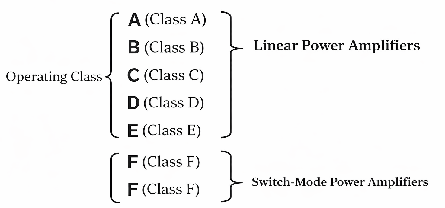
The working frequency of traditional linear power amplifiers is very high, but the relative frequency band is narrow. Radio frequency power amplifiers generally use frequency selection networks as load loops. Radio frequency power amplifiers can be divided into three types of working states: A (A), B (B) and C (C) according to the current conduction angle. The conduction angle of Class A amplifier current is 360°, which is suitable for low-power amplification of small signals. The conduction angle of Class B amplifier current is equal to 180°, and the conduction angle of Class C amplifier current is less than 180°. Both Class B and Class C are suitable for high-power working states, and the output power and efficiency of Class C working states are the highest among the three working states. Most radio frequency power amplifiers work in Class C, but the current waveform distortion of Class C amplifiers is too large to be used for tuning loops as load resonance power amplification. Because the tuning loop has filtering ability, the loop current and voltage are still close to the sinusoidal waveform, and the distortion is very small.
Switching Mode PA (SMPA) makes electronic devices work in the switching state. Common ones are D-type amplifiers and E-E-class amplifiers. The efficiency of D-class amplifiers is higher than that of C-class amplifiers. SMPA drives the active transistor into switching mode. The working state of the transistor is either on or off. There is no overlap in the time domain waveform of voltage and current, so the DC power consumption is zero, and the ideal efficiency can reach 100%.
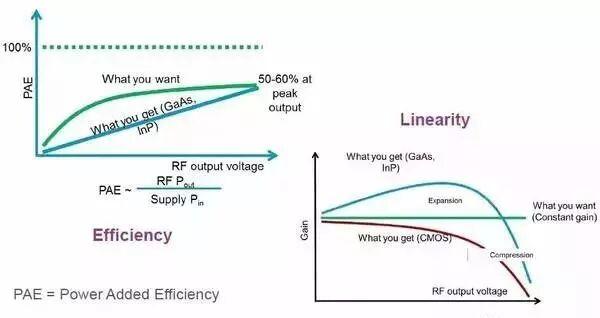
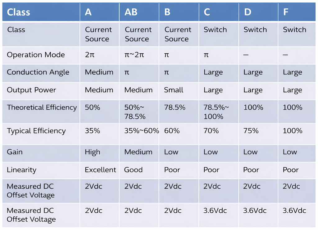
Traditional linear power amplifiers have high gain and linearity but low efficiency, while switching power amplifiers have high efficiency and high output power, but poor linearity. See the following table for details:
Circuit composition
There are different types of amplifiers. To simplify, the circuit of the amplifier can be composed of the following parts: transistor, bias and stability circuit, input and output matching circuit.
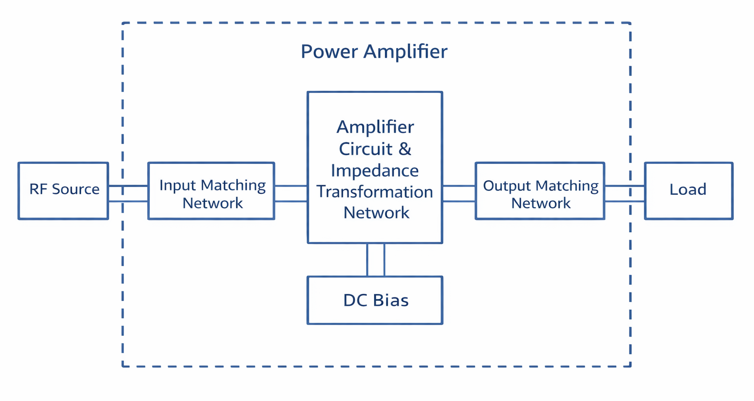
1-1. Transistor
There are many kinds of transistors, including the invention of transistors with various structures. In essence, the work of transistors is manifested as a controlled current source or voltage source, and its working mechanism is to convert the energy of DC without content into a “useful” output. DC energy is obtained from the outside world, which is consumed by transistors and converted into useful components. Different transistors have different “abilities”, such as their ability to withstand power, which is also due to the different ability to obtain DC energy; for example, its reaction speed is different, which determines how wide and high it can work in the frequency band; for example, its impedance towards the input and output ends is different, and the external response Different abilities determine the difficulty of matching it.
1-2. Bias and Stability Circuits
Bias and stability circuits serve different functions, but their design goals often overlap, so they can be discussed together. Transistors require a proper bias, called the quiescent point, which defines their operating mode and performance.
- Small variations in the bias point suit small-signal operation.
- Larger variations support high-power output.
- Low-demand points enable low-noise operation.
- Points near saturation create a switching state.
Choosing the correct bias point is essential for normal operation. In broadband or high-frequency amplifiers, the bias circuit significantly affects performance and should be considered part of the matching network.
Bias networks are either:
- Passive (self-bias): Simple resistor networks, sensitive to transistor variations and temperature.
- Active: Offers better stability and temperature performance, but increases circuit size, layout complexity, and power consumption.
Stability circuits are placed before the matching network to ensure the transistor operates smoothly and reliably. A transistor with a stability circuit is effectively a “stabilized” device ready for connection to external circuits.
1-3. Input and Output Matching Circuits
Matching circuits ensure efficient power transfer and optimize transistor performance. The design depends on the transistor type and desired outcome:
- Small transistors may intentionally limit signal reception to improve noise performance.
- Large power transistors require careful output design to avoid instability while preserving non-distorted energy.
Common impedance matching topologies:
- L-matching: Simple, two degrees of freedom (L and C). Q (bandwidth) is fixed once impedance ratio and frequency are set.
- π-matching: Absorbs parasitic capacitance, widely used in practical circuits.
- T-matching: Effective when parasitic inductance dominates, absorbing it into the network.
These matching networks balance gain, stability, and linearity to ensure optimal RF PA performance.
We’re committed to innovating RF solutions that empower your projects. Whether upgrading a network or designing new systems, consider the benefits outlined here to make informed choices. Contact us today to discover how our amplifiers can elevate your technology.