Newsroom
LDMOS RF Power Amplifier: Working Principles, Advantages, Applications, and Design Considerations
Laterally Diffused Metal Oxide Semiconductor (LDMOS) technology has been a dominant force in RF power amplification for decades, offering a balance of performance, cost, and reliability.
This article delves into the fundamentals of LDMOS RF power amplifiers, exploring their operation, benefits, comparisons with emerging alternatives like GaN, practical uses, design strategies, limitations, and future directions. Whether you’re an engineer optimizing base station efficiency or a researcher pushing the boundaries of RF systems, understanding LDMOS is essential for navigating today’s high-frequency landscape.
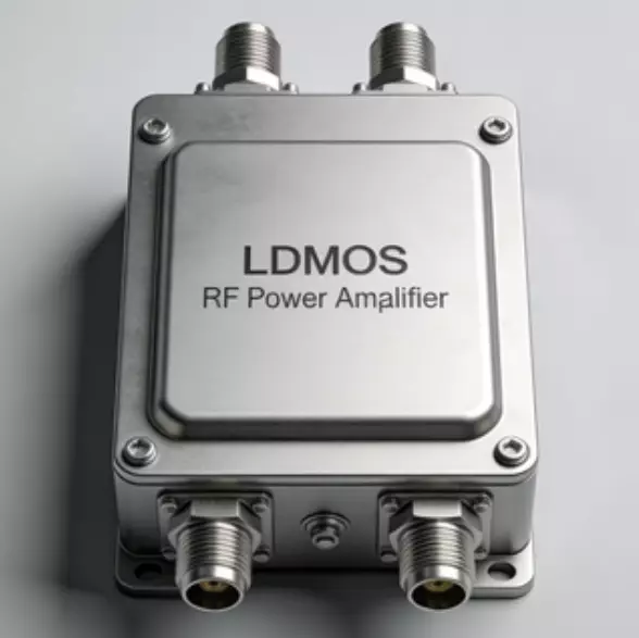
What Is an LDMOS RF Power Amplifier?
An LDMOS RF power amplifier is an electronic device designed to boost the power of radio frequency signals while maintaining signal integrity. At its core, it utilizes LDMOS transistors, which are silicon-based metal-oxide-semiconductor field-effect transistors (MOSFETs) optimized for high-power RF amplifier and high-frequency operations. Unlike standard MOSFETs, LDMOS features a lateral diffusion process that creates a drift region between the source and drain, enabling higher breakdown voltages and better power handling.
LDMOS transistors emerged in the 1990s as a solution for RF applications requiring robust performance. They are characterized by their ability to operate at frequencies up to several GHz, with power outputs ranging from watts to kilowatts. Key attributes include high power density (up to 2 W/mm for 50V variants), excellent linearity, and efficiency, making them ideal for amplification in wireless networks. These amplifiers convert low-power RF input signals into high-power outputs, essential for transmitting signals over long distances without distortion.
In structure, an LDMOS transistor consists of a source, gate, and drain on a silicon substrate. The lateral diffusion allows for a longer channel length, reducing short-channel effects and improving voltage tolerance. Compared to vertical MOSFETs, LDMOS offers easier integration into monolithic circuits, which is why it’s prevalent in base station power amplifiers. Today, LDMOS holds about 35% of the RF power semiconductor market, underscoring its maturity and widespread adoption.
How Does an LDMOS RF Power Amplifier Work?
The working principle of an LDMOS RF power amplifier revolves around controlled signal amplification through RF power amplifier transistor biasing and impedance matching. An input RF signal enters the amplifier, where it’s modulated by the LDMOS transistor. The gate voltage induces a depletion region, forming a conductive channel between source and drain. This channel allows current flow, amplifying the signal based on the transistor’s gain characteristics.
In operation, LDMOS amplifiers typically run in Class AB or Class C modes for efficiency. The drift region in LDMOS handles high voltages (up to 50V or more), preventing breakdown during peak power excursions. For instance, in a push-pull configuration, two LDMOS transistors alternate conduction, reducing distortion and improving efficiency. Harmonic tuning is crucial; appropriate load modulation ensures the amplifier operates at peak efficiency, often achieving 50-60% power-added efficiency (PAE) in tuned circuits.
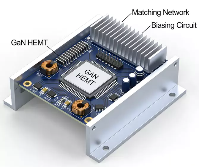
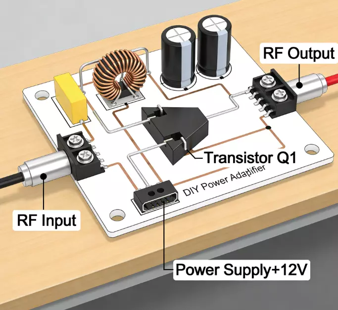
A typical LDMOS RF power amplifier circuit includes input matching networks (e.g., L-networks for impedance transformation), the transistor stage, and output matching to maximize power transfer. Biasing circuits maintain quiescent current, preventing thermal runaway. For high-power RF designs, like those exceeding 1 kW, envelope tracking adjusts bias dynamically to enhance linearity.
Here’s a simplified schematic of an LDMOS-based amplifier circuit for illustration:
Advantages of LDMOS RF Power Amplifiers
LDMOS RF power amplifiers offer several compelling advantages that have cemented their position in the industry. First, their high power density allows for compact designs, delivering up to 2 W/mm at 50V, far surpassing older technologies like bipolar junction transistors (BJTs). This density translates to smaller footprints in base stations, reducing overall system size and cost.
Efficiency is another key benefit; LDMOS can achieve 50-60% PAE in Class AB operation, minimizing power consumption and heat generation. Linearity is excellent, with low intermodulation distortion, making them suitable for multi-carrier signals in 4G/5G networks. Reliability under mismatch conditions is superior, withstanding VSWR up to 65:1 in rugged variants.
Cost-effectiveness stems from silicon-based manufacturing, leveraging mature CMOS processes for high yields. Unlike GaN, LDMOS doesn’t require exotic substrates, keeping prices low. Additionally, high breakdown voltage (over 100V) and low on-resistance enhance ruggedness, ideal for ISM and broadcast applications.
LDMOS vs GaN RF Power Amplifiers
When comparing LDMOS and GaN RF power amplifiers, the choice depends on frequency, efficiency, and cost. LDMOS excels below 3-4 GHz, offering mature, cost-effective solutions with good linearity. For example, 50V LDMOS provides 2 W/mm power density and 50-60% PAE at P1dB. It’s widely used in sub-6 GHz 5G due to lower parasitic capacitance and easier integration.
GaN, however, shines at higher frequencies (above 3 GHz), with 5-10 W/mm density and up to 70% PAE, enabling smaller, more efficient designs for mmWave and radar. GaN’s wide bandgap allows higher breakdown voltages and better thermal performance, but it requires more complex linearization (e.g., higher-order polynomials for predistortion) due to stronger nonlinearity. Cost-wise, LDMOS is cheaper (mature silicon process), while GaN-on-SiC is pricier but offers superior power at high freq.
In broadband RF power amplifier applications, GaN provides wider bandwidth with less matching complexity, but LDMOS remains dominant for narrowband cellular (e.g., 2G-4G). Thermal management is trickier for GaN due to higher power density, though its efficiency reduces overall heat.
Common Applications of LDMOS RF Power Amplifiers
LDMOS RF power amplifiers are ubiquitous in telecommunications, powering cellular base stations for 2G-5G networks. They handle multi-carrier signals in macro cells, ensuring reliable coverage. In broadcasting, they drive FM transmitters with high efficiency, supporting kilowatt-level outputs.
Industrial applications include RF heating and plasma generation, where LDMOS replaces magnetrons in microwave ovens and drying systems. Aerospace and defense use them in radars and ISM bands for their ruggedness. Emerging uses in RF energy for cooking and medical devices leverage their linearity.
In base stations, LDMOS amplifiers enable higher subscriber capacity through digital RF power amplifier modulation. Their integration in Doherty architectures boosts efficiency for variable loads.
Key Design Considerations for LDMOS RF Power Amplifiers
Designing an LDMOS RF power amplifier requires attention to impedance matching, thermal management, and linearity. Start backward from the output: Use L-networks or baluns for load matching to achieve desired power. Biasing circuit for RF power amplifier must account for temperature drift; thermistors stabilize quiescent current.
Thermal design is critical—use copper heat spreaders and fans, as junction temperatures above 150°C degrade reliability. For linearity, implement digital predistortion (DPD) to counter nonlinearity. Power combining techniques, like Wilkinson dividers, scale output for multi-device setups.
Shielding prevents oscillations, especially in cascaded stages. Consider safe operating area (SOA) to avoid hot carrier effects.
Challenges and Limitations of LDMOS Technology
Despite advantages of RF power amplifier, LDMOS faces challenges like current drift from temperature, causing gain variations. Hot carrier injection reduces long-term reliability, mitigated but not eliminated. At high frequencies (>4 GHz), efficiency drops due to parasitics.
Integration with sub-50nm processes is tricky, with scaling issues affecting yield. Reliability under radiation or ESD is a concern for aerospace. Compared to GaN, LDMOS has lower power density, limiting mmWave use.
Future Trends in LDMOS RF Power Amplifier Technology
Looking ahead, LDMOS will evolve alongside GaN, with hybrids combining both for optimal performance. GaN-on-Si may displace LDMOS in sub-6 GHz by 2028, but LDMOS persists in cost-sensitive apps. Advances in 300mm wafers and DPD will boost efficiency to 60%+.
6G trials demand higher linearity; LDMOS with AI-driven predistortion could adapt. Sustainability pushes eco-friendly designs, like GaN/LDMOS for energy-efficient 5G. Market growth projects RF amplifiers to $15B by 2031, with LDMOS at 9.7% CAGR.
This market forecast chart illustrates the trajectory:
Conclusion
LDMOS RF power amplifiers remain a vital technology, balancing performance and affordability in RF systems. From base stations to industrial heating, their versatility endures despite emerging challengers like GaN. By addressing design considerations and limitations, engineers can harness LDMOS for future innovations in 5G and beyond. As the RF landscape shifts, LDMOS’s evolution ensures its relevance in powering tomorrow’s connected world-just contact us!