Newsroom
GaN RF Power Amplifier: Benefits, Applications, Design Considerations, and Technology Overview
In the rapidly evolving field of radio frequency (RF) technology, GaN RF power amplifiers have emerged as a cornerstone for high-performance applications. These devices leverage gallium nitride (GaN) semiconductors to deliver superior power handling, efficiency, and bandwidth compared to traditional alternatives.
As demands for faster data rates, longer transmission distances, and more compact systems grow, understanding the intricacies of GaN RF power amplifiers becomes essential for engineers and system designers.
What Is a GaN RF Power Amplifier?
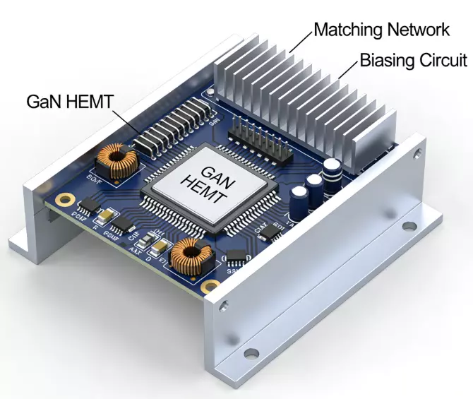
A GaN RF power amplifier is an electronic device designed to amplify RF signals using transistors based on gallium nitride material. At its core, it typically employs a high-electron-mobility transistor (HEMT) structure, where a heterojunction between GaN and aluminum gallium nitride (AlGaN) creates a two-dimensional electron gas (2DEG) channel. This channel enables high electron mobility and saturation velocity, allowing the amplifier to operate at high frequencies and power levels.
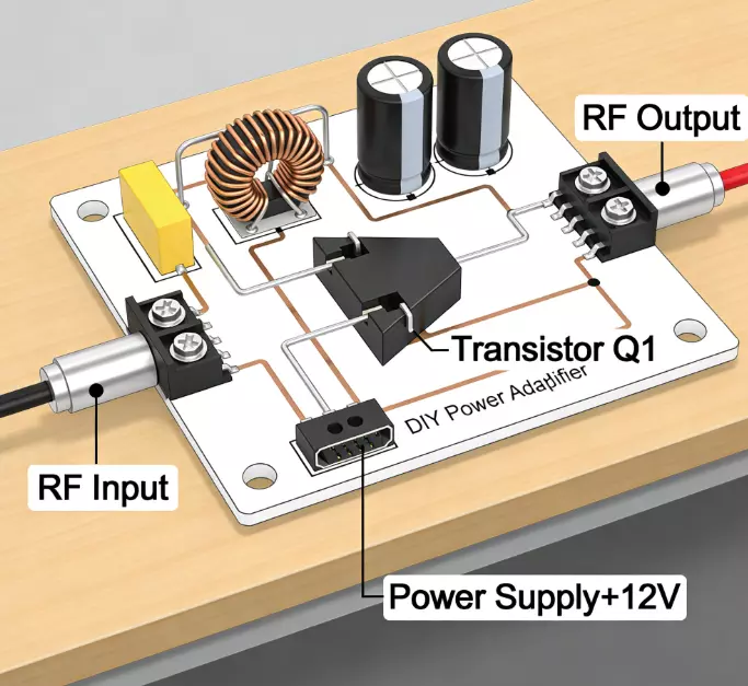
Unlike silicon-based amplifiers, GaN devices are wide-bandgap semiconductors with a bandgap of approximately 3.4 eV. This property permits operation at elevated voltages and temperatures without breakdown. A typical GaN RF power amplifier consists of input matching networks, the GaN transistor itself, output matching RF power amplifier circuits, and bias networks. The RF power amplifier transistor is often grown on a silicon carbide (SiC) substrate for enhanced thermal dissipation, though silicon (Si) substrates are used for cost-sensitive applications.
In practice, GaN RF power amplifiers can deliver output powers ranging from watts to kilowatts, depending on the configuration. For instance, in monolithic microwave integrated circuits (MMICs), multiple stages are integrated to achieve gain levels exceeding 20 dB across broadband frequencies. The RF power amplifier design often incorporates class-AB or class-F topologies to optimize efficiency.
Why Are GaN RF Power Amplifiers Important?
GaN RF power amplifiers play a pivotal role in modern communication and sensing systems due to their ability to handle high power densities while maintaining efficiency. In an era dominated by 5G and emerging 6G networks, these amplifiers enable massive multiple-input multiple-output (MIMO) systems, where dozens of antennas require compact, high-efficiency power sources. Without GaN technology, achieving the required signal strength for long-range coverage in base stations would demand larger, less efficient hardware, increasing operational costs and energy consumption.
Beyond telecommunications, GaN RF power amplifiers are crucial in defense and aerospace, powering radar systems that detect threats over vast distances. Their importance of RF power amplifier stems from the need for reliable performance in harsh environments, such as high-altitude satellites or military vehicles, where thermal and electrical stresses are extreme. As global data traffic surges—projected to increase by 50% annually—GaN amplifiers ensure networks can scale without proportional increases in power usage.
Moreover, they contribute to sustainability by reducing cooling requirements in data centers and base stations. Traditional amplifiers might dissipate 60% of input power as heat, whereas GaN devices can achieve power-added efficiencies (PAE) of 40-60%, directly lowering carbon footprints. In essence, GaN RF power amplifiers are indispensable for advancing wireless infrastructure, enabling innovations like autonomous vehicles and smart cities.
Key Advantages of GaN RF Power Amplifiers
GaN RF power amplifiers offer several key advantages that set them apart in high-frequency applications. Foremost is their exceptional power density, typically ranging from 4-8 W/mm, which is significantly higher than alternatives like GaAs (0.5-1.5 W/mm). This allows for smaller die sizes while delivering equivalent or greater output power, facilitating compact designs in space-constrained systems.
Efficiency is another standout benefit of RF power amplifier. GaN amplifiers routinely achieve PAE levels of 40-60% at frequencies up to 40 GHz, outperforming silicon-based options by 20-30%. This efficiency translates to lower operating costs and reduced thermal management needs, as less input power is wasted as heat. GaN’s high breakdown voltage—exceeding 100V—enables operation at 28-48V biases, reducing current draw and simplifying power supply designs.
Wide bandwidth operation is a critical edge, with GaN supporting octave or broader frequency ranges without retuning. This versatility is ideal for multi-band systems. Additionally, GaN’s superior thermal conductivity (390-490 W/m·K on SiC substrates) enhances reliability in high-power scenarios, extending mean time to failure (MTTF).
In RF systems, GaN also provides better linearity, minimizing distortion in modulated signals, which is vital for 5G’s high data rates. Overall, these advantages make GaN RF power amplifiers a preferred choice for demanding applications, balancing performance, size, and cost-effectiveness.
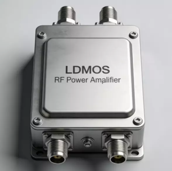
GaN vs LDMOS vs GaAs RF Power Amplifiers
When comparing GaN, LDMOS, and GaAs RF power amplifiers, several metrics highlight their strengths and trade-offs. GaN excels in high-frequency and high-power scenarios, offering power densities of 4-8 W/mm and efficiencies up to 70% at P1dB. It operates effectively above 4 GHz, with breakdown voltages over 100V, making it ideal for 5G and radar.
LDMOS, based on silicon, is cost-effective and rugged, handling mismatches up to 65:1 VSWR. It delivers high power (up to 1500W CW) below 4 GHz with efficiencies around 50-60%, but struggles at higher frequencies due to lower electron mobility. GaAs, meanwhile, suits low-power, high-frequency applications (up to 100 GHz) with good linearity but limited power density (0.5-1.5 W/mm) and efficiencies of 40-50%. Its lower breakdown voltage (20-40V) restricts high-power RF power amplifier use.
GaN’s superior performance comes at a higher cost, but for broadband RF power amplifier, high-efficiency needs, it outperforms LDMOS in infrastructure and GaAs in power-handling. This chart visually compares the power-frequency capabilities of GaN, LDMOS, and GaAs technologies.
Applications of GaN RF Power Amplifiers
GaN RF power amplifiers find extensive use across diverse sectors due to their robust performance. In telecommunications, they power 5G base stations and massive MIMO arrays, enabling high-speed data transmission with output powers exceeding 100W per channel. Their wide bandwidth supports sub-6 GHz and mmWave bands, crucial for urban coverage and low-latency applications like IoT.
In defense and aerospace, GaN amplifiers drive phased-array radars for missile detection and electronic warfare systems, offering pulse powers up to kilowatts with high PAE to minimize battery drain in portable units. Satellite communications benefit from GaN’s efficiency in VSAT terminals and onboard transponders, where size and power constraints are critical.
Other applications include medical imaging (e.g., MRI RF coils), industrial heating, and automotive radar for advanced driver-assistance systems (ADAS). In data centers, GaN enables high-power mmWave links for backhaul, reducing latency. As 5G deployment accelerates, GaN’s role in small cells and repeaters ensures seamless connectivity in dense environments.
GaN RF Power Amplifier Design Considerations
Designing GaN RF power amplifiers requires careful attention to several factors to optimize performance. Bias sequencing is paramount: the gate voltage (typically -2 to -5V) must be applied before the drain (28-50V) to prevent damage from self-bias effects. Vgs drift, caused by trapping phenomena, necessitates compensation circuits to maintain stable operation under RF drive.
Thermal management is critical, given GaN’s high power density. Designers should use SiC substrates and incorporate via arrays in PCBs to dissipate heat, targeting junction temperatures below 200°C for longevity. Matching networks—often microstrip or lumped elements—must account for GaN’s high input impedance, using tools like Smith charts for broadband matching.
Linearity enhancements, such as digital predistortion (DPD), address nonlinearities in high-PAPR signals. Power scalability involves paralleling transistors with Wilkinson combiners. Finally, reliability RF power amplifier testing under accelerated conditions ensures MTTF exceeds 10^6 hours.
Challenges of GaN RF Power Amplifiers
Despite their advantages, GaN RF power amplifiers face notable challenges. High fabrication costs arise from complex epitaxial growth and the need for specialized substrates like SiC, making them 2-3 times more expensive than LDMOS equivalents. This limits adoption in cost-sensitive markets.
Reliability issues, such as gate leakage and trap-induced current collapse, can degrade performance over time, requiring rigorous testing and derating. Thermal challenges persist; while GaN has good conductivity, high densities demand advanced cooling, complicating system integration.
Design complexity is another hurdle: impedance matching at high frequencies is tricky, and bias sensitivity can lead to oscillations. Supply chain vulnerabilities, including GaN material shortages, pose risks. Addressing these through process improvements is ongoing, but they remain barriers to widespread use.
The Future of GaN RF Power Amplifier Technology
The future of GaN RF power amplifier technology is promising, driven by advancements in multichannel transistors and integration. Innovations like superlattice castellated field effect transistors (SLCFETs) promise output power densities exceeding current limits, enhancing linearity for 6G mmWave systems.
Cost reductions through GaN-on-Si processes will broaden accessibility, while AI-assisted design—using reinforcement learning for optimization—will streamline development. Expect higher frequencies (up to 100 GHz) for satellite and automotive radar, with efficiencies approaching 80% via advanced topologies.
Market growth is projected at 15.9% CAGR, reaching $3.5 billion by 2033, fueled by 5G/6G and defense needs.
Conclusion
GaN RF power amplifiers represent a transformative technology, offering unmatched benefits in power, efficiency, and versatility. From telecommunications to defense, their applications continue to expand, despite design and cost challenges. As RF power amplifier manufacturer like ZR Hi-Tech push boundaries, the future holds even greater innovations, solidifying GaN’s role in next-generation RF systems–just contact us!