Newsroom
Bias Circuit for RF Power Amplifiers: Design Principles, Types, and Best Practices
In the world of radio frequency (RF) technology, power amplifiers are essential components that boost signal strength for applications ranging from wireless communications to radar systems. As an RF power amplifier manufacturer, we understand that the bias circuit plays a pivotal role in ensuring optimal performance.
This circuit sets the operating point of the amplifier’s transistors, influencing efficiency, linearity, and stability. In this in-depth guide, we’ll explore the fundamentals of bias circuits, their importance, common methods, and best practices for design and evaluation.
What Is a Bias Circuit in an RF Power Amplifier?
A bias circuit in an RF power amplifier is a network of components that establishes the DC operating conditions for the active devices, typically transistors such as BJTs, FETs, or GaN HEMTs. It applies a steady-state voltage or current to the transistor’s input (base or gate) to position the quiescent point on the device’s characteristic curve. This setup allows the amplifier to handle AC signals effectively without distortion or inefficiency.
At its core, the bias circuit isolates the DC supply from the RF signal path while preventing RF leakage into the power supply. For instance, in a basic setup, resistors, diodes, or inductors are used to control the base-emitter voltage in BJTs or gate-source voltage in FETs. Without proper biasing, the amplifier could operate in cutoff, saturation, or nonlinear regions, leading to poor gain, high distortion, or even device failure.
In practical terms, bias circuits can be passive (using resistors and capacitors) or active (incorporating transistors or op-amps for stability). Passive circuits are simple and cost-effective but sensitive to temperature variations, while active ones provide better control over quiescent current (I_Q).
Why Is Proper Biasing Critical for RF Power Amplifier Performance?
Proper biasing is fundamental to achieving balanced performance in RF power amplifiers. It directly impacts key metrics like gain, efficiency, linearity, and thermal stability. For example, incorrect biasing can cause thermal runaway in RF power amplifier transistors, where increasing temperature leads to higher current, further heating the device until failure.
Linearity is crucial for minimizing distortion in modulated signals, such as those in 5G or Wi-Fi systems. Biasing ensures the amplifier operates in its linear region, reducing intermodulation distortion (IMD) and harmonics. Efficiency, measured as power-added efficiency (PAE), is another critical factor—poor biasing wastes power as heat, reducing battery life in portable devices or increasing cooling requirements in base stations.
Stability is also at stake; unstable biasing can lead to oscillations, especially at high frequencies. Temperature variations exacerbate these issues, as RF power amplifier key transistor parameters like V_BE shift with heat (typically -2.5 mV/°C for BJTs). Proper biasing incorporates compensation to maintain consistent performance across operating conditions.
In high-power RF power amplifier applications, such as radar or satellite communications, biasing affects output power and reliability. Over-biasing increases power consumption, while under-biasing limits output swing. Studies show that optimized biasing can improve PAE by 10-20%, extending system range and reducing costs.
Common Biasing Methods Used in RF Power Amplifiers
Several biasing methods are employed in RF power amplifiers, each suited to specific requirements. The choice depends on factors like RF power amplifier class, frequency, and power level.
- Base-Biased Emitter Feedback: This uses a base resistor (R_B) and emitter resistor (R_E) to stabilize current. As temperature rises, collector current increases, dropping more voltage across R_E and reducing base current. It’s simple but wastes power in R_E and reduces AC gain unless bypassed with a capacitor.
- Voltage-Divider Emitter Feedback: A resistor divider sets the base voltage, with emitter feedback for stability. It offers better temperature compensation than base-biased methods and is common in Class A amplifiers.
- Collector Feedback: The collector voltage feeds back to the base via a resistor, self-adjusting the bias. It’s low-cost but less stable over temperature variations.
- Diode Feedback: Diodes mounted on the transistor’s heatsink track temperature changes, adjusting forward voltage to compensate for V_BE shifts. This is effective for high-frequency designs where emitter resistors are avoided.
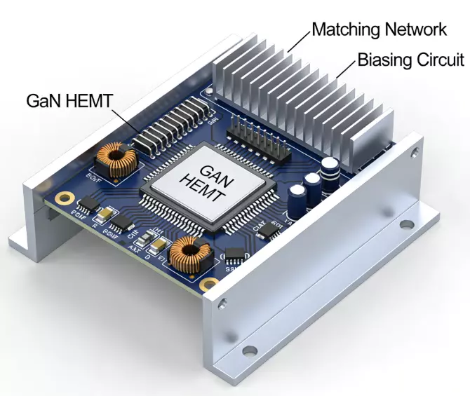
- Active Feedback Bias: Uses transistors in a current mirror or op-amp configuration for precise control. Ideal for GaN or LDMOS devices requiring negative gate bias and sequencing to prevent damage.
Active methods are preferred for modern amplifiers due to their adjustability and stability.
Bias Circuits for Different RF Power Amplifier Classes
RF power amplifiers are classified by conduction angle, which determines biasing needs.
- Class A: Biased at midpoint for 360° conduction. Offers high linearity but low efficiency (25-35%). Bias circuits maintain constant current, often using active feedback to fix the operating point regardless of RF drive.
- Class B: 180° conduction, biased at cutoff. More efficient (up to 78.5%) but introduces crossover distortion. Push-pull configurations with diode compensation minimize this.
- Class AB: Conduction between 180°-360°, balancing linearity and efficiency (50-70%). Bias circuits use temperature-compensated networks to prevent thermal runaway.
- Class C: Less than 180° conduction, highly efficient (80-90%) but nonlinear. Often uses self-bias or negative bias for pulsed applications like radar.
The illustration below shows conduction angles for these classes. Class selection influences bias complexity—Class A needs stable current sources, while Class C can use simpler grounding via inductors.
How to Design a Bias Circuit for an RF Power Amplifier
Designing a bias circuit involves several steps:
- Determine Operating Point: Select I_Q and V_CE (or V_DS) based on datasheet for desired gain, linearity, and efficiency. For example, in a GaN HEMT, set gate voltage for optimal PAE.
- Choose Bias Method: Match to amplifier class and requirements. Use simulation tools like SPICE to model temperature effects.
- Incorporate Isolation: Use inductors and capacitors in a bias tee to separate DC and RF paths. The inductor blocks RF, while the capacitor blocks DC.
- Add Sequencing: For depletion-mode devices like GaN, apply negative gate bias before drain voltage to avoid damage.
- Simulate and Optimize: Evaluate for stability, using S-parameters to check for oscillations.
Temperature Compensation and Stability in RF Bias Circuits
Temperature fluctuations can shift bias points, degrading performance. Compensation techniques include:
- Diode Compensation: Diodes mimic transistor V_BE changes, adjusting bias voltage.
- Thermistor Networks: NTC thermistors reduce voltage with rising temperature.
- Active Compensation: Op-amps or bandgap references maintain constant I_Q.
Stability ensures no oscillations; use bypass capacitors and ferrite beads to dampen resonances. In GaN amps, adaptive biasing senses temperature and adjusts gate voltage.
Bias Circuit Design Challenges and Common Mistakes
Challenges include balancing efficiency and linearity, managing parasitics at high frequencies, and ensuring sequencing. Common mistakes:
- Ignoring Temperature Effects: Leads to drift or runaway.
- Poor Isolation: RF leakage into DC supply causes instability.
- Incorrect Sequencing: Damages GaN devices.
- Overlooking Parasitics: Stray capacitance lowers self-resonant frequency.
Illustrating common errors:
- Avoid by thorough simulation and prototyping.
Practical Examples of Bias Circuits in RF Power Amplifiers
- Class AB GaN PA: Uses active bias with current mirror for stable I_Q. Example: Gate biased at -2.5V, drain at 28V, with thermistor compensation.
- Class C BJT PA: Self-bias via inductor to ground, suitable for pulsed radar.
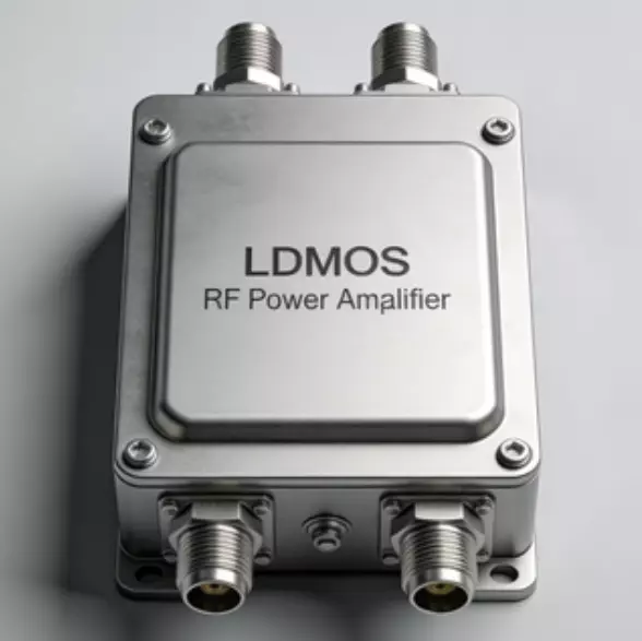
- LDMOS Base Station Amp: Diode feedback on heatsink tracks temperature, maintaining linearity.
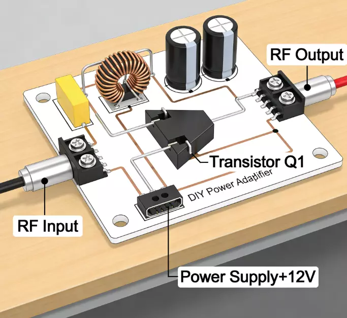
Practical circuit examples:
- These ensure reliable operation in real-world scenarios.
How to Choose or Evaluate a Bias Circuit for RF Power Amplifiers
To choose:
- Assess Requirements: Linearity vs. efficiency, frequency range.
- Evaluate Stability: Check for oscillations via S-parameters.
- Test RF power amplifier Efficiency: Measure PAE under load.
- Simulate Variations: Temperature, supply noise.
Use tools like LTSpice for evaluation. Prioritize active bias for high-performance needs.
Conclusion
Bias circuits are the unsung heroes of RF power amplifiers, enabling efficient, linear, and stable operation. By understanding RF power amplifier design principles, types, and best practices, engineers can optimize systems for demanding applications.
Whether passive or active, the right bias circuit enhances performance and reliability, ensuring your RF designs excel in a competitive landscape—contact us to learn how our solutions can power your next project.